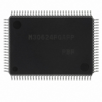
M30624FGAFP#U3 Renesas Electronics America, M30624FGAFP#U3 Datasheet - Page 150

M30624FGAFP#U3
Manufacturer Part Number
M30624FGAFP#U3
Description
IC M16C MCU FLASH 100QFP
Manufacturer
Renesas Electronics America
Series
M16C™ M16C/60r
Datasheets
1.M30622SAFPU5.pdf
(277 pages)
2.M30622SAFPU5.pdf
(617 pages)
3.M30622SAFPU5.pdf
(308 pages)
Specifications of M30624FGAFP#U3
Core Processor
M16C/60
Core Size
16-Bit
Speed
16MHz
Connectivity
SIO, UART/USART
Peripherals
DMA, PWM, WDT
Number Of I /o
85
Program Memory Size
256KB (256K x 8)
Program Memory Type
FLASH
Ram Size
20K x 8
Voltage - Supply (vcc/vdd)
4.2 V ~ 5.5 V
Data Converters
A/D 10x10b, D/A 2x8b
Oscillator Type
Internal
Operating Temperature
-40°C ~ 85°C
Package / Case
100-QFP
For Use With
867-1000 - KIT QUICK START RENESAS 62PM3062PT3-CPE-3 - EMULATOR COMPACT M16C/62P/30P
Lead Free Status / RoHS Status
Lead free / RoHS Compliant
Eeprom Size
-
Available stocks
Company
Part Number
Manufacturer
Quantity
Price
Part Number:
M30624FGAFP#U3M30624FGAFP#D3
Manufacturer:
Renesas Electronics America
Quantity:
10 000
Part Number:
M30624FGAFP#U3M30624FGAFP#D5
Manufacturer:
Renesas Electronics America
Quantity:
10 000
- Current page: 150 of 277
- Download datasheet (4Mb)
S I/O3, 4
Figure 1.16.33. Timing chart for setting S
Figure 1.16.34. S I/Oi operation timing chart
Signal written to the S I/Oi
transmit/receive register
Note 1: With the internal clock selected for the transfer clock, the frequency dividing ratio can be selected using bits 0 and 1 of the S I/Oi control
Note 2: With the internal clock selected for the transfer clock, the S
Note 3: Shown above is the case where the S
SI/Oi interrupt request
bit
(Example) With “H” selected for S
S I/Oi output S
Signal written to the S I/Oi
transmit/receive register
When using an external clock for the transfer clock, the S
time can be set to the high or the low state. Figure 1.16.33 shows the timing chart for setting an S
initial value and how to set it.
Figure 1.16.34 shows the S I/Oi operation timing
SI/Oi internal clock
S I/Oi input S
Functions for setting an S
S I/Oi operation timing
S
register. (i=3,4) (No frequency division, 8-division frequency, 32-division frequency.)
OUT
S I/Oi port select bit
Transfer clock
S
OUT
i terminal output
Note: The set value is output only when the external clock has been selected. When
(i = 3, 4)
S
i's initial value
OUT
set bit (SMi7)
(Note 1)
(i= 3, 4)
(i= 3, 4)
(i= 3, 4)
i (internal)
initializing S
If the internal clock has been selected or if S
this output goes to the high-impedance state.
OUT
IN
(SMi3)
i
i
"H"
"L"
"H"
"L"
"H"
"H"
"H"
"L"
"L"
"L"
"1"
"0"
OUT
Port output
Setting the S
i, make sure the CLKi pin input is held “H” level.
initial value to H
1.5 cycle (max)
OUT
OUT
OUT
i:
Hiz
OUT
i
i (i = 3, 4) port select bit =“1”.
Port selection
(normal port
i initial value
D
Initial value = “H” (Note)
OUT
0
OUT
output disable has been set,
OUT
i’s initial value and how to set it
S
i (i = 3, 4) pin becomes to the high-impedance state after the transfer finishes.
D
OUT
1
i)
D
2
D0
D0
OUTi
D
3
pin output level during a non-transfer
SINGLE-CHIP 16-BIT CMOS MICROCOMPUTER
D
4
stored data in the S I/Oi transmission/
(Port select: Normal port
Signal written to the S I/Oi register
S I/Oi port select bit SMi3 = 0
(S
SOUTi initial value select bit
S
S
D
OUT
OUT
OUT
5
S I/Oi port select bit
=“L”
reception register
i: Internal
i terminal = Outputting
i terminal = “H” output
SMi3 = 0
(Falling edge)
SMi7 = 1
M16C / 62A Group
D
6
Mitsubishi microcomputers
“H”
“H” level)
1
“L”
D
7
S
OUT
Note2
i)
Hiz
OUTi
147
Related parts for M30624FGAFP#U3
Image
Part Number
Description
Manufacturer
Datasheet
Request
R

Part Number:
Description:
KIT STARTER FOR M16C/29
Manufacturer:
Renesas Electronics America
Datasheet:

Part Number:
Description:
KIT STARTER FOR R8C/2D
Manufacturer:
Renesas Electronics America
Datasheet:

Part Number:
Description:
R0K33062P STARTER KIT
Manufacturer:
Renesas Electronics America
Datasheet:

Part Number:
Description:
KIT STARTER FOR R8C/23 E8A
Manufacturer:
Renesas Electronics America
Datasheet:

Part Number:
Description:
KIT STARTER FOR R8C/25
Manufacturer:
Renesas Electronics America
Datasheet:

Part Number:
Description:
KIT STARTER H8S2456 SHARPE DSPLY
Manufacturer:
Renesas Electronics America
Datasheet:

Part Number:
Description:
KIT STARTER FOR R8C38C
Manufacturer:
Renesas Electronics America
Datasheet:

Part Number:
Description:
KIT STARTER FOR R8C35C
Manufacturer:
Renesas Electronics America
Datasheet:

Part Number:
Description:
KIT STARTER FOR R8CL3AC+LCD APPS
Manufacturer:
Renesas Electronics America
Datasheet:

Part Number:
Description:
KIT STARTER FOR RX610
Manufacturer:
Renesas Electronics America
Datasheet:

Part Number:
Description:
KIT STARTER FOR R32C/118
Manufacturer:
Renesas Electronics America
Datasheet:

Part Number:
Description:
KIT DEV RSK-R8C/26-29
Manufacturer:
Renesas Electronics America
Datasheet:

Part Number:
Description:
KIT STARTER FOR SH7124
Manufacturer:
Renesas Electronics America
Datasheet:

Part Number:
Description:
KIT STARTER FOR H8SX/1622
Manufacturer:
Renesas Electronics America
Datasheet:

Part Number:
Description:
KIT DEV FOR SH7203
Manufacturer:
Renesas Electronics America
Datasheet:


