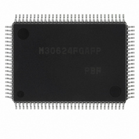
M30624FGAFP#U3 Renesas Electronics America, M30624FGAFP#U3 Datasheet - Page 123

M30624FGAFP#U3
Manufacturer Part Number
M30624FGAFP#U3
Description
IC M16C MCU FLASH 100QFP
Manufacturer
Renesas Electronics America
Series
M16C™ M16C/60r
Datasheets
1.M30622SAFPU5.pdf
(277 pages)
2.M30622SAFPU5.pdf
(617 pages)
3.M30622SAFPU5.pdf
(308 pages)
Specifications of M30624FGAFP#U3
Core Processor
M16C/60
Core Size
16-Bit
Speed
16MHz
Connectivity
SIO, UART/USART
Peripherals
DMA, PWM, WDT
Number Of I /o
85
Program Memory Size
256KB (256K x 8)
Program Memory Type
FLASH
Ram Size
20K x 8
Voltage - Supply (vcc/vdd)
4.2 V ~ 5.5 V
Data Converters
A/D 10x10b, D/A 2x8b
Oscillator Type
Internal
Operating Temperature
-40°C ~ 85°C
Package / Case
100-QFP
For Use With
867-1000 - KIT QUICK START RENESAS 62PM3062PT3-CPE-3 - EMULATOR COMPACT M16C/62P/30P
Lead Free Status / RoHS Status
Lead free / RoHS Compliant
Eeprom Size
-
Available stocks
Company
Part Number
Manufacturer
Quantity
Price
Part Number:
M30624FGAFP#U3M30624FGAFP#D3
Manufacturer:
Renesas Electronics America
Quantity:
10 000
Part Number:
M30624FGAFP#U3M30624FGAFP#D5
Manufacturer:
Renesas Electronics America
Quantity:
10 000
- Current page: 123 of 277
- Download datasheet (4Mb)
Clock synchronous serial I/O mode
120
Table 1.16.4. Input/output pin functions in clock synchronous serial I/O mode
(when transfer clock output from multiple pins is not selected)
TxDi
(P6
RxDi
(P6
CLKi
(P6
CTSi/RTSi
(P6
Pin name
Table 1.16.4 lists the functions of the input/output pins during clock synchronous serial I/O mode. This
table shows the pin functions when the transfer clock output from multiple pins function is not selected.
Note that for a period from when the UARTi operation mode is selected to when transfer starts, the TxDi
pin outputs an “H”. (If the N-channel open-drain is selected, this pin is in floating state.)
3
0
2
1
, P6
, P6
, P6
, P6
7
5
4
6
, P7
, P7
, P7
, P7
0
1
2
3
)
)
)
)
RTS output
Serial data output
Serial data input
Transfer clock output
Transfer clock input
CTS input
Programmable I/O port
Function
(Outputs dummy data when performing reception only)
Port P6
bit 1 at address 03EF
(Can be used as an input port when performing transmission only)
Internal/external clock select bit (bit 3 at address 03A0
Internal/external clock select bit (bit 3 at address 03A0
Port P6
bit 2 at address 03EF
CTS/RTS disable bit (bit 4 at address 03A4
CTS/RTS disable bit (bit 4 at address 03A4
CTS/RTS function select bit (bit 2 at address 03A4
Port P6
bit 3 at address 03EF
CTS/RTS disable bit (bit 4 at address 03A4
CTS/RTS function select bit (bit 2 at address 03A4
2
1
0
, P6
, P6
, P6
6
5
4
and P7
and P7
and P7
1
2
16
16
3
16
direction register (bits 2 and 6 at address 03EE
direction register (bits 1 and 5 at address 03EE
direction register (bits 0 and 4 at address 03EE
)= “0”
) = “0”
) = “0”
Method of selection
SINGLE-CHIP 16-BIT CMOS MICROCOMPUTER
16
16
16
, 03AC
, 03AC
, 03AC
16
16
16
16
16
, 03AC
, 03AC
, 037C
, 037C
16
16
, 037C
, 03A8
, 03A8
M16C / 62A Group
16
16
Mitsubishi microcomputers
16
16)
16
, 037C
, 037C
16
16
) = “1”
) =“0”
= “0”
, 0378
, 0378
16
16
16
16
) = “0”
16
) = “1”
16
16
,
,
,
) = “0”
) = “1”
Related parts for M30624FGAFP#U3
Image
Part Number
Description
Manufacturer
Datasheet
Request
R

Part Number:
Description:
KIT STARTER FOR M16C/29
Manufacturer:
Renesas Electronics America
Datasheet:

Part Number:
Description:
KIT STARTER FOR R8C/2D
Manufacturer:
Renesas Electronics America
Datasheet:

Part Number:
Description:
R0K33062P STARTER KIT
Manufacturer:
Renesas Electronics America
Datasheet:

Part Number:
Description:
KIT STARTER FOR R8C/23 E8A
Manufacturer:
Renesas Electronics America
Datasheet:

Part Number:
Description:
KIT STARTER FOR R8C/25
Manufacturer:
Renesas Electronics America
Datasheet:

Part Number:
Description:
KIT STARTER H8S2456 SHARPE DSPLY
Manufacturer:
Renesas Electronics America
Datasheet:

Part Number:
Description:
KIT STARTER FOR R8C38C
Manufacturer:
Renesas Electronics America
Datasheet:

Part Number:
Description:
KIT STARTER FOR R8C35C
Manufacturer:
Renesas Electronics America
Datasheet:

Part Number:
Description:
KIT STARTER FOR R8CL3AC+LCD APPS
Manufacturer:
Renesas Electronics America
Datasheet:

Part Number:
Description:
KIT STARTER FOR RX610
Manufacturer:
Renesas Electronics America
Datasheet:

Part Number:
Description:
KIT STARTER FOR R32C/118
Manufacturer:
Renesas Electronics America
Datasheet:

Part Number:
Description:
KIT DEV RSK-R8C/26-29
Manufacturer:
Renesas Electronics America
Datasheet:

Part Number:
Description:
KIT STARTER FOR SH7124
Manufacturer:
Renesas Electronics America
Datasheet:

Part Number:
Description:
KIT STARTER FOR H8SX/1622
Manufacturer:
Renesas Electronics America
Datasheet:

Part Number:
Description:
KIT DEV FOR SH7203
Manufacturer:
Renesas Electronics America
Datasheet:


