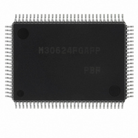
M30624FGAFP#U3 Renesas Electronics America, M30624FGAFP#U3 Datasheet - Page 245

M30624FGAFP#U3
Manufacturer Part Number
M30624FGAFP#U3
Description
IC M16C MCU FLASH 100QFP
Manufacturer
Renesas Electronics America
Series
M16C™ M16C/60r
Datasheets
1.M30622SAFPU5.pdf
(277 pages)
2.M30622SAFPU5.pdf
(617 pages)
3.M30622SAFPU5.pdf
(308 pages)
Specifications of M30624FGAFP#U3
Core Processor
M16C/60
Core Size
16-Bit
Speed
16MHz
Connectivity
SIO, UART/USART
Peripherals
DMA, PWM, WDT
Number Of I /o
85
Program Memory Size
256KB (256K x 8)
Program Memory Type
FLASH
Ram Size
20K x 8
Voltage - Supply (vcc/vdd)
4.2 V ~ 5.5 V
Data Converters
A/D 10x10b, D/A 2x8b
Oscillator Type
Internal
Operating Temperature
-40°C ~ 85°C
Package / Case
100-QFP
For Use With
867-1000 - KIT QUICK START RENESAS 62PM3062PT3-CPE-3 - EMULATOR COMPACT M16C/62P/30P
Lead Free Status / RoHS Status
Lead free / RoHS Compliant
Eeprom Size
-
Available stocks
Company
Part Number
Manufacturer
Quantity
Price
Part Number:
M30624FGAFP#U3M30624FGAFP#D3
Manufacturer:
Renesas Electronics America
Quantity:
10 000
Part Number:
M30624FGAFP#U3M30624FGAFP#D5
Manufacturer:
Renesas Electronics America
Quantity:
10 000
- Current page: 245 of 277
- Download datasheet (4Mb)
Appendix Standard Serial I/O Mode 1 (Flash Memory Version)
242
Figure 1.29.5. Timing for clearing the status register
Figure 1.29.6. Timing for the page program
Clear Status Register Command
Page Program Command
This command clears the bits (SR3–SR5) which are set when the status register operation ends in
error. When the “50
When the clear status register operation ends, the RTS
“L” level.
This command writes the specified page (256 bytes) in the flash memory sequentially one byte at a
time. Execute the page program command as explained here following.
When reception setup for the next 256 bytes ends, the RTS
the “L” level. The result of the page program can be known by reading the status register. For more
information, see the section on the status register.
Each block can be write-protected with the lock bit. For more information, see the section on the data
protection function. Additional writing is not allowed with already programmed pages.
(M16C reception data)
(1) Transfer the “41
(2) Transfer addresses A
(3) From the 4th byte onward, as write data (D
(M16C transmit data)
A
8
to A
RTS1(BUSY)
23
is input sequentially from the smallest address first, that page is automatically written.
CLK1
RxD1
TxD1
16
(M16C reception data)
” command code is sent with the 1st byte, the aforementioned bits are cleared.
16
(M16C transmit data)
” command code with the 1st byte.
8
to A
RTS1(BUSY)
15
41
and A
16
CLK1
RxD1
TxD1
A
16
A
8
15
to A
to
0
23
–D
A
A
16
with the 2nd and 3rd bytes respectively.
7
23
) for the page (256 bytes) specified with addresses
to
50
16
1
data0
(BUSY) signal changes from the “H” to the
1
(BUSY) signal changes from the “H” to
SINGLE-CHIP 16-BIT CMOS MICROCOMPUTER
data255
M16C / 62A Group
Mitsubishi microcomputers
Related parts for M30624FGAFP#U3
Image
Part Number
Description
Manufacturer
Datasheet
Request
R

Part Number:
Description:
KIT STARTER FOR M16C/29
Manufacturer:
Renesas Electronics America
Datasheet:

Part Number:
Description:
KIT STARTER FOR R8C/2D
Manufacturer:
Renesas Electronics America
Datasheet:

Part Number:
Description:
R0K33062P STARTER KIT
Manufacturer:
Renesas Electronics America
Datasheet:

Part Number:
Description:
KIT STARTER FOR R8C/23 E8A
Manufacturer:
Renesas Electronics America
Datasheet:

Part Number:
Description:
KIT STARTER FOR R8C/25
Manufacturer:
Renesas Electronics America
Datasheet:

Part Number:
Description:
KIT STARTER H8S2456 SHARPE DSPLY
Manufacturer:
Renesas Electronics America
Datasheet:

Part Number:
Description:
KIT STARTER FOR R8C38C
Manufacturer:
Renesas Electronics America
Datasheet:

Part Number:
Description:
KIT STARTER FOR R8C35C
Manufacturer:
Renesas Electronics America
Datasheet:

Part Number:
Description:
KIT STARTER FOR R8CL3AC+LCD APPS
Manufacturer:
Renesas Electronics America
Datasheet:

Part Number:
Description:
KIT STARTER FOR RX610
Manufacturer:
Renesas Electronics America
Datasheet:

Part Number:
Description:
KIT STARTER FOR R32C/118
Manufacturer:
Renesas Electronics America
Datasheet:

Part Number:
Description:
KIT DEV RSK-R8C/26-29
Manufacturer:
Renesas Electronics America
Datasheet:

Part Number:
Description:
KIT STARTER FOR SH7124
Manufacturer:
Renesas Electronics America
Datasheet:

Part Number:
Description:
KIT STARTER FOR H8SX/1622
Manufacturer:
Renesas Electronics America
Datasheet:

Part Number:
Description:
KIT DEV FOR SH7203
Manufacturer:
Renesas Electronics America
Datasheet:


