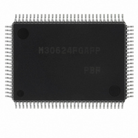
M30624FGAFP#U3 Renesas Electronics America, M30624FGAFP#U3 Datasheet - Page 149

M30624FGAFP#U3
Manufacturer Part Number
M30624FGAFP#U3
Description
IC M16C MCU FLASH 100QFP
Manufacturer
Renesas Electronics America
Series
M16C™ M16C/60r
Datasheets
1.M30622SAFPU5.pdf
(277 pages)
2.M30622SAFPU5.pdf
(617 pages)
3.M30622SAFPU5.pdf
(308 pages)
Specifications of M30624FGAFP#U3
Core Processor
M16C/60
Core Size
16-Bit
Speed
16MHz
Connectivity
SIO, UART/USART
Peripherals
DMA, PWM, WDT
Number Of I /o
85
Program Memory Size
256KB (256K x 8)
Program Memory Type
FLASH
Ram Size
20K x 8
Voltage - Supply (vcc/vdd)
4.2 V ~ 5.5 V
Data Converters
A/D 10x10b, D/A 2x8b
Oscillator Type
Internal
Operating Temperature
-40°C ~ 85°C
Package / Case
100-QFP
For Use With
867-1000 - KIT QUICK START RENESAS 62PM3062PT3-CPE-3 - EMULATOR COMPACT M16C/62P/30P
Lead Free Status / RoHS Status
Lead free / RoHS Compliant
Eeprom Size
-
Available stocks
Company
Part Number
Manufacturer
Quantity
Price
Part Number:
M30624FGAFP#U3M30624FGAFP#D3
Manufacturer:
Renesas Electronics America
Quantity:
10 000
Part Number:
M30624FGAFP#U3M30624FGAFP#D5
Manufacturer:
Renesas Electronics America
Quantity:
10 000
- Current page: 149 of 277
- Download datasheet (4Mb)
S I/O3, 4
146
Note 1: n is a value from 00
Note 2: With the external clock selected:
Note 3: If the internal clock is used for the synchronous clock, the transfer clock signal stops at the “H” state.
Table 1.16.13. Specifications of S I/O3, 4
Transfer data format
Transfer clock
Conditions for
transmission/
reception start
Interrupt request
generation timing
Select function
Precaution
• Before data can be written to the SI/Oi transmit/receive register (addresses 0360
• The S I/Oi circuit keeps on with the shift operation as long as the synchronous clock is entered in it,
CLKi pin input must be in the high state. Also, before rewriting the SI/Oi Control Register (addresses
0362
so stop the synchronous clock at the instant when it counts to eight. The internal clock, if selected,
automatically stops.
Item
16
, 0366
16
)’s bit 7 (S
• Transfer data length: 8 bits
• With the internal clock selected (bit 6 of 0362
• With the external clock selected (bit 6 of 0362
• To start transmit/reception, the following requirements must be met:
• To use S I/Oi interrupts, the following requirements must be met:
• Rising edge of the last transfer clock. (Note 3)
• LSB first or MSB first selection
• Function for setting an S
• Unlike UART0–2, SI/Oi (i = 3, 4) is not divided for transfer register and buffer.
• When the internal clock is selected for the transfer clock, S
f
- Select the synchronous clock (use bit 6 of 0362
- S
- S I/Oi port select bit (bit 3 of 0362
- Select the transfer direction (use bit 5 of 0362
-Write transfer data to SI/Oi transmit/receive register (0360
- Clear the SI/Oi interrupt request bit before writing transfer data to the SI/Oi
Whether transmission/reception begins with bit 0 (LSB) or bit 7 (MSB) can be
selected.
When using an external clock for the transfer clock, the user can choose the
S
Figure 1.16.33.
Therefore, do not write the next transfer data to the SI/Oi transmit/receive register
(addresses 0360
for a 1/2 transfer clock period after it finished transferring and then goes to a high-
impedance state. However, if the transfer data is written to the SI/Oi transmit/
receive register (addresses 0360
the high-impedance state immediately upon writing and the data hold time is
thereby reduced.
8
Select a frequency dividing ratio if the internal clock has been selected (use bits
0 and 1 of 0362
transmit/receive register (bit 3 of 0049
OUT
/2(ni+1), f
16
OUT
through FF
i pin output level during a non-transfer time. For details on how to set, see
i initial value set bit (use bit 7 of 0362
OUT
32
i initial value set bit), make sure the CLKi pin input is held high.
/2(ni+1) (Note 1)
16
16
16
set in the S I/Oi bit rate generator (i = 3, 4).
, 0364
, 0366
OUT
16
16
) during a transfer.
).
i initial value selection
Specifications
16
16
, 0364
16
, 0366
, 0366
16
, 0048
16
16
) during this time, S
16
16
16
SINGLE-CHIP 16-BIT CMOS MICROCOMPUTER
) = 1.
= 0):Input from the CLKi terminal (Note 2)
, 0366
, 0366
16
16
16
, 0366
) = 0.
, 0366
16
16
)= 1.
16
= “1”): f
16
OUT
)
).
16
i holds the last data
, 0364
M16C / 62A Group
OUT
1
/2(ni+1),
Mitsubishi microcomputers
16
i is placed in
, 0364
16
)
16
), the
Related parts for M30624FGAFP#U3
Image
Part Number
Description
Manufacturer
Datasheet
Request
R

Part Number:
Description:
KIT STARTER FOR M16C/29
Manufacturer:
Renesas Electronics America
Datasheet:

Part Number:
Description:
KIT STARTER FOR R8C/2D
Manufacturer:
Renesas Electronics America
Datasheet:

Part Number:
Description:
R0K33062P STARTER KIT
Manufacturer:
Renesas Electronics America
Datasheet:

Part Number:
Description:
KIT STARTER FOR R8C/23 E8A
Manufacturer:
Renesas Electronics America
Datasheet:

Part Number:
Description:
KIT STARTER FOR R8C/25
Manufacturer:
Renesas Electronics America
Datasheet:

Part Number:
Description:
KIT STARTER H8S2456 SHARPE DSPLY
Manufacturer:
Renesas Electronics America
Datasheet:

Part Number:
Description:
KIT STARTER FOR R8C38C
Manufacturer:
Renesas Electronics America
Datasheet:

Part Number:
Description:
KIT STARTER FOR R8C35C
Manufacturer:
Renesas Electronics America
Datasheet:

Part Number:
Description:
KIT STARTER FOR R8CL3AC+LCD APPS
Manufacturer:
Renesas Electronics America
Datasheet:

Part Number:
Description:
KIT STARTER FOR RX610
Manufacturer:
Renesas Electronics America
Datasheet:

Part Number:
Description:
KIT STARTER FOR R32C/118
Manufacturer:
Renesas Electronics America
Datasheet:

Part Number:
Description:
KIT DEV RSK-R8C/26-29
Manufacturer:
Renesas Electronics America
Datasheet:

Part Number:
Description:
KIT STARTER FOR SH7124
Manufacturer:
Renesas Electronics America
Datasheet:

Part Number:
Description:
KIT STARTER FOR H8SX/1622
Manufacturer:
Renesas Electronics America
Datasheet:

Part Number:
Description:
KIT DEV FOR SH7203
Manufacturer:
Renesas Electronics America
Datasheet:


