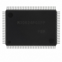
M30624FGAFP#U3 Renesas Electronics America, M30624FGAFP#U3 Datasheet - Page 225

M30624FGAFP#U3
Manufacturer Part Number
M30624FGAFP#U3
Description
IC M16C MCU FLASH 100QFP
Manufacturer
Renesas Electronics America
Series
M16C™ M16C/60r
Datasheets
1.M30622SAFPU5.pdf
(277 pages)
2.M30622SAFPU5.pdf
(617 pages)
3.M30622SAFPU5.pdf
(308 pages)
Specifications of M30624FGAFP#U3
Core Processor
M16C/60
Core Size
16-Bit
Speed
16MHz
Connectivity
SIO, UART/USART
Peripherals
DMA, PWM, WDT
Number Of I /o
85
Program Memory Size
256KB (256K x 8)
Program Memory Type
FLASH
Ram Size
20K x 8
Voltage - Supply (vcc/vdd)
4.2 V ~ 5.5 V
Data Converters
A/D 10x10b, D/A 2x8b
Oscillator Type
Internal
Operating Temperature
-40°C ~ 85°C
Package / Case
100-QFP
For Use With
867-1000 - KIT QUICK START RENESAS 62PM3062PT3-CPE-3 - EMULATOR COMPACT M16C/62P/30P
Lead Free Status / RoHS Status
Lead free / RoHS Compliant
Eeprom Size
-
Available stocks
Company
Part Number
Manufacturer
Quantity
Price
Part Number:
M30624FGAFP#U3M30624FGAFP#D3
Manufacturer:
Renesas Electronics America
Quantity:
10 000
Part Number:
M30624FGAFP#U3M30624FGAFP#D5
Manufacturer:
Renesas Electronics America
Quantity:
10 000
CPU Rewrite Mode (Flash Memory Version)
222
Precautions on CPU Rewrite Mode
Described below are the precautions to be observed when rewriting the flash memory in CPU rewrite
mode.
(1) Operation speed
(2) Instructions inhibited against use
(3) Interrupts inhibited against use
(4) Internal reserved area expansion bit (Bit 3 at address 0005
(5) Reset
(6) Access disable
(7) How to access
During CPU rewrite mode, set the BCLK as shown below using the main clock divide ratio select bit
(bit 6 at address 0006
6.25 MHz or less when wait bit (bit 7 at address 0005
12.5 MHz or less when wait bit (bit 7 at address 0005
The instructions listed below cannot be used during CPU rewrite mode because they refer to the
internal data of the flash memory:
UND instruction, INTO instruction, JMPS instruction, JSRS instruction, and BRK instruction
The address match interrupt cannot be used during CPU rewrite mode because they refer to the
internal data of the flash memory. If interrupts have their vector in the variable vector table, they can be
used by transferring the vector into the RAM area. The NMI and watchdog timer interrupts can be
used because the flash memory conterol register 0 and 1 is forcibly initialized and return to normal
mode when each interrupt occurs. But it is needed that the jump addresses for each interrupt are set
in the fixed vector table and there is an interrupt program. Since the rewrite operation is halted when
the NMI and watchdog timer interrupts occur, it is needed that CPU rewriting mode select bit is set to
“1” and the erase/program operation is performed over again.
The reserved area of the internal memory can be changed by using the internal reserved area expan-
sion bit (bit 3 at address 0005
is set to 1, the internal reserved area expansion bit (bit 3 at address 0005
cally. Similarly, if the CPU rewrite mode select bit (bit 1 at address 03B7
reserved area expansion bit (bit 3 at address 0005
The precautions above apply to the products which RAM size is over 15 Kbytes or flash memory size
is over 192 Kbytes.
Reset input is always accepted. After a reset, the addresses 0C0000
a reserved area and cannot be accessed. Therefore, if your product has this area in the user ROM
area, do not write any address of this area to the reset vector. This area is made accessible by
changing the internal reserved area expansion bit (bit 3 at address 0005
Write CPU rewrite mode select bit, flash memory power supply-OFF bit and user ROM area select bit
only when executing out of an area other than the internal flash memory.
For CPU rewrite mode select bit, lock bit disable select bit, and flash memory power supply-OFF bit to
be set to “1”, the user needs to write a “0” and then a “1” to it in succession. When it is not this
procedure, it is not enacted in “1”. This is necessary to ensure that no interrupt or DMA transfer will be
executed during the interval.
Write CPU rewrite mode select bit only when executing out of an area other than the internal flash
memory. Also only when NMI pin is “H” level.
_______
16
and bits 6 and 7 at address 0007
_______
16
). However, if the CPU rewrite mode select bit (bit 1 at address 03B7
16
) also is set to 0 automatically.
16
16
) = 0 (without internal access wait state)
) = 1 (with internal access wait state)
_______
16
):
SINGLE-CHIP 16-BIT CMOS MICROCOMPUTER
16
)
16
through 0CFFFF
16
16
16
) in a program.
) also is set to 1 automati-
) is set to 0, the internal
M16C / 62A Group
Mitsubishi microcomputers
16
are made
16
)


