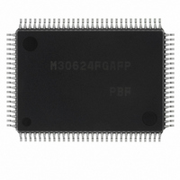
M30624FGAFP#U3 Renesas Electronics America, M30624FGAFP#U3 Datasheet - Page 222

M30624FGAFP#U3
Manufacturer Part Number
M30624FGAFP#U3
Description
IC M16C MCU FLASH 100QFP
Manufacturer
Renesas Electronics America
Series
M16C™ M16C/60r
Datasheets
1.M30622SAFPU5.pdf
(277 pages)
2.M30622SAFPU5.pdf
(617 pages)
3.M30622SAFPU5.pdf
(308 pages)
Specifications of M30624FGAFP#U3
Core Processor
M16C/60
Core Size
16-Bit
Speed
16MHz
Connectivity
SIO, UART/USART
Peripherals
DMA, PWM, WDT
Number Of I /o
85
Program Memory Size
256KB (256K x 8)
Program Memory Type
FLASH
Ram Size
20K x 8
Voltage - Supply (vcc/vdd)
4.2 V ~ 5.5 V
Data Converters
A/D 10x10b, D/A 2x8b
Oscillator Type
Internal
Operating Temperature
-40°C ~ 85°C
Package / Case
100-QFP
For Use With
867-1000 - KIT QUICK START RENESAS 62PM3062PT3-CPE-3 - EMULATOR COMPACT M16C/62P/30P
Lead Free Status / RoHS Status
Lead free / RoHS Compliant
Eeprom Size
-
Available stocks
Company
Part Number
Manufacturer
Quantity
Price
Part Number:
M30624FGAFP#U3M30624FGAFP#D3
Manufacturer:
Renesas Electronics America
Quantity:
10 000
Part Number:
M30624FGAFP#U3M30624FGAFP#D5
Manufacturer:
Renesas Electronics America
Quantity:
10 000
Mitsubishi microcomputers
M16C / 62A Group
SINGLE-CHIP 16-BIT CMOS MICROCOMPUTER
CPU Rewrite Mode (Flash Memory Version)
Outline Performance (CPU Rewrite Mode)
In the CPU rewrite mode, the CPU erases, programs and reads the internal flash memory as instructed by
software commands. Operations must be executed from a memory other than the internal flash memory,
such as the internal RAM.
When the CPU rewrite mode select bit (bit 1 at address 03B7
) is set to “1”, transition to CPU rewrite mode
16
occurs and software commands can be accepted.
In the CPU rewrite mode, write to and read from software commands and data into even-numbered ad-
dress (“0” for byte address A
) in 16-bit units. Always write 8-bit software commands into even-numbered
0
address. Commands are ignored with odd-numbered addresses.
Use software commands to control program and erase operations. Whether a program or erase operation
has terminated normally or in error can be verified by reading the status register.
Figure 1.26.1 shows the flash memory control register 0 and the flash memory control register 1.
_____
Bit 0 of the flash memory control register 0 is the RY/BY status flag used exclusively to read the operating
status of the flash memory. During programming and erase operations, it is “0”. Otherwise, it is “1”.
Bit 1 of the flash memory control register 0 is the CPU rewrite mode select bit. The CPU rewrite mode is
entered by setting this bit to “1”, so that software commands become acceptable. In CPU rewrite mode, the
CPU becomes unable to access the internal flash memory directly. Therefore, write bit 1 in an area other
_______
than the internal flash memory. Also only when NMI pin is "H" level. To set this bit to “1”, it is necessary to
write “0” and then write “1” in succession. The bit can be set to “0” by only writing a “0” .
Bit 2 of the flash memory control register 0 is a lock bit disable select bit. By setting this bit to “1”, it is
possible to disable erase and write protect (block lock) effectuated by the lock bit data. The lock bit disable
select bit only disables the lock bit function; it does not change the lock data bit value. However, if an erase
operation is performed when this bit =“1”, the lock bit data that is “0” (locked) is set to “1” (unlocked) after
erasure. To set this bit to “1”, it is necessary to write “0” and then write “1” in succession. This bit can be
manipulated only when the CPU rewrite mode select bit = “1”.
Bit 3 of the flash memory control register 0 is the flash memory reset bit used to reset the control circuit of
the internal flash memory. This bit is used when exiting CPU rewrite mode and when flash memory access
has failed. When the CPU rewrite mode select bit is “1”, writing “1” for this bit resets the control circuit. To
release the reset, it is necessary to set this bit to “0”.
Bit 5 of the flash memory control register 0 is a user ROM area select bit which is effective in only boot
mode. If this bit is set to “1” in boot mode, the area to be accessed is switched from the boot ROM area to
the user ROM area. When the CPU rewrite mode needs to be used in boot mode, set this bit to “1”. Note
that if the microcomputer is booted from the user ROM area, it is always the user ROM area that can be
accessed and this bit has no effect. When in boot mode, the function of this bit is effective regardless of
whether the CPU rewrite mode is on or off. Write to this bit only when executing out of an area other than
the internal flash memory.
Bit 3 of the flash memory control register 1 turns power supply to the internal flash memory on/off. When
this bit is set to “1”, power is not supplied to the internal flash memory, thus power consumption can be
reduced. However, in this state, the internal flash memory cannot be accessed. To set this bit to “1”, it is
necessary to write “0” and then write “1” in succession. Use this bit mainly in the low speed mode (when
X
is the count source of BCLK).
CIN
When the CPU is shifted to the stop or wait modes, power to the internal flash memory is automatically shut
off. It is reconnected automatically when CPU operation is restored. Therefore, it is not particularly neces-
sary to set flash memory control register 1.
219


