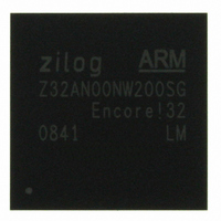
Z32AN00NW200SG Zilog, Z32AN00NW200SG Datasheet - Page 157

Z32AN00NW200SG
Manufacturer Part Number
Z32AN00NW200SG
Description
IC ARM922T MCU 200MHZ 256-BGA
Manufacturer
Zilog
Series
Encore!® 32r
Datasheet
1.Z32AN00NW200SG.pdf
(196 pages)
Specifications of Z32AN00NW200SG
Core Processor
ARM9
Core Size
16/32-Bit
Speed
200MHz
Connectivity
EBI/EMI, IrDA, SmartCard, SPI, UART/USART, USB OTG
Peripherals
DMA, LCD, Magnetic Card Reader, POR, PWM, WDT
Number Of I /o
76
Program Memory Type
ROMless
Ram Size
64K x 8
Voltage - Supply (vcc/vdd)
1.71 V ~ 3.6 V
Data Converters
A/D 4x10b
Oscillator Type
Internal
Operating Temperature
-40°C ~ 85°C
Package / Case
256-LBGA
For Use With
269-4713 - KIT DEV ENCORE 32 SERIES
Lead Free Status / RoHS Status
Lead free / RoHS Compliant
Eeprom Size
-
Program Memory Size
-
Other names
269-4717
Available stocks
Company
Part Number
Manufacturer
Quantity
Price
- Current page: 157 of 196
- Download datasheet (4Mb)
Z32AN Series Data Sheet
18.1 Operation
18.2 Signals
18.2.1 Master-In/Slave-Out (MISO)
18.2.2 Master-Out/Slave-In (MOSI)
18.2.3 Serial Clock (SCK)
DS0200-003
The SPI is a full-duplex, synchronous, character-oriented channel that supports a four-wire interface (serial
clock, transmit, receive, and Slave select). The SPI block consists of a transmit/receive shift register
(supported by FIFOs), a Baud Rate (clock) Generator, and a control unit.
During an SPI transfer, data is sent and received simultaneously by both the Master and the Slave SPI
devices. Separate signals are required for data and serial clock. When an SPI transfer occurs, a multi-bit
(selectable from 1 to 16-bit) character is shifted out on one data pin and a multi-bit character is
simultaneously shifted in on a second data pin. A 16-bit shift register in the Master and another 16-bit shift
register in the Slave are connected as a circular buffer with the most significant bit (bit 15) sent first.
The SPI contains two 4x16 FIFOs to support the transmit and receive directions. New data is moved
automatically from the transmit FIFO into the shift register at the start of every new SPI transfer as long as
there is data in the transmit FIFO. At the end of every SPI transfer, the data is then moved from the shift
register to the receive FIFO.
The SPI signals are reset to GPIO inputs. An external pull-up resistor must be used to prevent floating input
signals especially for the clock and slave select.
This pin is configured as input of the master and output of the slave. It is one of the two lines that transfer
serial data, with the most significant bit sent first. The MISO pin of a slave device is placed in a high-
impedance state if the Slave is not selected. When SPI is not enabled, this signal is in a high-impedance
state.
This pin is configured as an output in of the master and an input of the slave. It is one of the two lines that
transfer serial data, with the most significant bit sent first. When SPI is not enabled, this signal is in a high-
impedance state.
This is used to synchronize data through MOSI and MISO. In master mode, the SPI’s Baud Rate Generator
creates the serial clock. The Master drives the serial clock out its own SCK pin to the Slave’s SCK pin.
When the SPI is configured as a Slave, the SCK pin is an input and the clock signal from the Master
synchronizes the data transfer between the Master and Slave devices. Slave devices ignore the SCK signal,
unless the nSS pin is asserted. When configured as a Slave, the SPI block requires a minimum SCK period
of greater than or equal to 8 times the hclk period.
The Master and Slave are each capable of exchanging a character of data during a sequence of NUMBITS
clock cycles (SPI_MOD.NUMBITS). In both master and slave devices, data is shifted on one edge of the
Figure 18-3: SPI Configured as a Slave
Page 144
Related parts for Z32AN00NW200SG
Image
Part Number
Description
Manufacturer
Datasheet
Request
R

Part Number:
Description:
Communication Controllers, ZILOG INTELLIGENT PERIPHERAL CONTROLLER (ZIP)
Manufacturer:
Zilog, Inc.
Datasheet:

Part Number:
Description:
KIT DEV FOR Z8 ENCORE 16K TO 64K
Manufacturer:
Zilog
Datasheet:

Part Number:
Description:
KIT DEV Z8 ENCORE XP 28-PIN
Manufacturer:
Zilog
Datasheet:

Part Number:
Description:
DEV KIT FOR Z8 ENCORE 8K/4K
Manufacturer:
Zilog
Datasheet:

Part Number:
Description:
KIT DEV Z8 ENCORE XP 28-PIN
Manufacturer:
Zilog
Datasheet:

Part Number:
Description:
DEV KIT FOR Z8 ENCORE 4K TO 8K
Manufacturer:
Zilog
Datasheet:

Part Number:
Description:
CMOS Z8 microcontroller. ROM 16 Kbytes, RAM 256 bytes, speed 16 MHz, 32 lines I/O, 3.0V to 5.5V
Manufacturer:
Zilog, Inc.
Datasheet:

Part Number:
Description:
Low-cost microcontroller. 512 bytes ROM, 61 bytes RAM, 8 MHz
Manufacturer:
Zilog, Inc.
Datasheet:

Part Number:
Description:
Z8 4K OTP Microcontroller
Manufacturer:
Zilog, Inc.
Datasheet:

Part Number:
Description:
CMOS SUPER8 ROMLESS MCU
Manufacturer:
Zilog, Inc.
Datasheet:

Part Number:
Description:
SL1866 CMOSZ8 OTP Microcontroller
Manufacturer:
Zilog, Inc.
Datasheet:

Part Number:
Description:
SL1866 CMOSZ8 OTP Microcontroller
Manufacturer:
Zilog, Inc.
Datasheet:

Part Number:
Description:
OTP (KB) = 1, RAM = 125, Speed = 12, I/O = 14, 8-bit Timers = 2, Comm Interfaces Other Features = Por, LV Protect, Voltage = 4.5-5.5V
Manufacturer:
Zilog, Inc.
Datasheet:

Part Number:
Description:
Manufacturer:
Zilog, Inc.
Datasheet:


