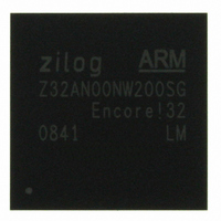
Z32AN00NW200SG Zilog, Z32AN00NW200SG Datasheet - Page 44

Z32AN00NW200SG
Manufacturer Part Number
Z32AN00NW200SG
Description
IC ARM922T MCU 200MHZ 256-BGA
Manufacturer
Zilog
Series
Encore!® 32r
Datasheet
1.Z32AN00NW200SG.pdf
(196 pages)
Specifications of Z32AN00NW200SG
Core Processor
ARM9
Core Size
16/32-Bit
Speed
200MHz
Connectivity
EBI/EMI, IrDA, SmartCard, SPI, UART/USART, USB OTG
Peripherals
DMA, LCD, Magnetic Card Reader, POR, PWM, WDT
Number Of I /o
76
Program Memory Type
ROMless
Ram Size
64K x 8
Voltage - Supply (vcc/vdd)
1.71 V ~ 3.6 V
Data Converters
A/D 4x10b
Oscillator Type
Internal
Operating Temperature
-40°C ~ 85°C
Package / Case
256-LBGA
For Use With
269-4713 - KIT DEV ENCORE 32 SERIES
Lead Free Status / RoHS Status
Lead free / RoHS Compliant
Eeprom Size
-
Program Memory Size
-
Other names
269-4717
Available stocks
Company
Part Number
Manufacturer
Quantity
Price
- Current page: 44 of 196
- Download datasheet (4Mb)
Z32AN Series Data Sheet
7.1.2
DS0200-003
The programmable timing associated with the single reads and writes are shown below. The example
provided here has settings of N
hclk is the reference for cycle timing.
Back-to-back accesses will be performed with the chip select remaining constantly active, if the timing of the
requests and the programmed parameters allow it.
Asynchronous Single Read and Write Transactions
Symbol
t
t
t
t
t
t
t
RWI
WS
WA
WH
RH
RS
RA
Equation
- or -
- or -
Table 7-2: Single Read/Write Timing (based on MEMC_TIMN)
Figure 7-2: Single Read/Write Timing Diagram
RS
=3, N
Description
Read Cycle Setup Time: Specifies the number of half clock cycles of setup
time before nOE goes active during a read cycle. Also, this specifies setup time
for A and nCS as well as provides time for D to go high-Z.
Read Access Time: Specifies the number of clock cycles before data is
samples and nOE returns to inactive.
Read Cycle hold Time: Specifies the number of clocks that OEn is inactive
before the end of the read cycle. This time is increased by a half clock if
N
Read/Write Idle Time: Specifies the minimum number of clocks after a read
before a subsequent write cycle, access on a different chip select, or data bus
clamping can occur.
Write Cycle Setup Time: Specifies the number of half clock cycles of setup
time before nWE goes active during a write cycle. Also, this specifies setup time
for A, D and nCS.
Write Access Time: Specifies the number of clock cycles before data is
sampled and nOE returns to inactive.
Write Cycle Hold Time: Specifies the number of clocks that OEn is inactive
before the end of the write cycle. This time is increased by a half clock if
N
RS
WS
[0]=1.
[0]=1.
RA
=3, N
RH
=1, N
WS
=3, N
WA
=3, N
WH
=1, N
RWI
and READY ignored.
Page 31
Related parts for Z32AN00NW200SG
Image
Part Number
Description
Manufacturer
Datasheet
Request
R

Part Number:
Description:
Communication Controllers, ZILOG INTELLIGENT PERIPHERAL CONTROLLER (ZIP)
Manufacturer:
Zilog, Inc.
Datasheet:

Part Number:
Description:
KIT DEV FOR Z8 ENCORE 16K TO 64K
Manufacturer:
Zilog
Datasheet:

Part Number:
Description:
KIT DEV Z8 ENCORE XP 28-PIN
Manufacturer:
Zilog
Datasheet:

Part Number:
Description:
DEV KIT FOR Z8 ENCORE 8K/4K
Manufacturer:
Zilog
Datasheet:

Part Number:
Description:
KIT DEV Z8 ENCORE XP 28-PIN
Manufacturer:
Zilog
Datasheet:

Part Number:
Description:
DEV KIT FOR Z8 ENCORE 4K TO 8K
Manufacturer:
Zilog
Datasheet:

Part Number:
Description:
CMOS Z8 microcontroller. ROM 16 Kbytes, RAM 256 bytes, speed 16 MHz, 32 lines I/O, 3.0V to 5.5V
Manufacturer:
Zilog, Inc.
Datasheet:

Part Number:
Description:
Low-cost microcontroller. 512 bytes ROM, 61 bytes RAM, 8 MHz
Manufacturer:
Zilog, Inc.
Datasheet:

Part Number:
Description:
Z8 4K OTP Microcontroller
Manufacturer:
Zilog, Inc.
Datasheet:

Part Number:
Description:
CMOS SUPER8 ROMLESS MCU
Manufacturer:
Zilog, Inc.
Datasheet:

Part Number:
Description:
SL1866 CMOSZ8 OTP Microcontroller
Manufacturer:
Zilog, Inc.
Datasheet:

Part Number:
Description:
SL1866 CMOSZ8 OTP Microcontroller
Manufacturer:
Zilog, Inc.
Datasheet:

Part Number:
Description:
OTP (KB) = 1, RAM = 125, Speed = 12, I/O = 14, 8-bit Timers = 2, Comm Interfaces Other Features = Por, LV Protect, Voltage = 4.5-5.5V
Manufacturer:
Zilog, Inc.
Datasheet:

Part Number:
Description:
Manufacturer:
Zilog, Inc.
Datasheet:


