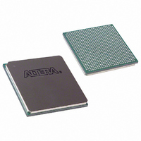
EP1S20F780I6N Altera, EP1S20F780I6N Datasheet - Page 349

EP1S20F780I6N
Manufacturer Part Number
EP1S20F780I6N
Description
IC STRATIX FPGA 20K LE 780-FBGA
Manufacturer
Altera
Series
Stratix®r
Specifications of EP1S20F780I6N
Number Of Logic Elements/cells
18460
Number Of Labs/clbs
1846
Total Ram Bits
1669248
Number Of I /o
586
Voltage - Supply
1.425 V ~ 1.575 V
Mounting Type
Surface Mount
Operating Temperature
-40°C ~ 100°C
Package / Case
780-FBGA
Family Name
Stratix
Number Of Logic Blocks/elements
18460
# I/os (max)
586
Frequency (max)
450.05MHz
Process Technology
0.13um (CMOS)
Operating Supply Voltage (typ)
1.5V
Logic Cells
18460
Ram Bits
1669248
Operating Supply Voltage (min)
1.425V
Operating Supply Voltage (max)
1.575V
Operating Temp Range
-40C to 100C
Operating Temperature Classification
Industrial
Mounting
Surface Mount
Pin Count
780
Package Type
FC-FBGA
Lead Free Status / RoHS Status
Lead free / RoHS Compliant
Number Of Gates
-
Lead Free Status / Rohs Status
Compliant
Available stocks
Company
Part Number
Manufacturer
Quantity
Price
Company:
Part Number:
EP1S20F780I6N
Manufacturer:
ALTERA
Quantity:
3 000
- Current page: 349 of 864
- Download datasheet (11Mb)
Clocking
Altera Corporation
July 2005
Note to
(1)
GNDA_PLL9
GNDG_PLL9
VCCA_PLL10
VCCG_PLL10
GNDA_PLL10
GNDG_PLL10
Table 1–13. Fast PLL Pins (Part 3 of 3)
PLLs 3, 4, 9, and 10 are not available on Stratix GX devices for general-purpose configuration. These PLLs are part
of the HSSI block. See AN 236: Using Source-Synchronous Signaling with DPA in Stratix GX Devices for more
information.
Table
Pin
1–13:
Stratix and Stratix GX devices provide a hierarchical clock structure and
multiple PLLs with advanced features. The large number of clocking
resources in combination with the clock synthesis precision provided by
enhanced and fast PLLs provides a complete clock management solution.
Global & Hierarchical Clocking
Stratix and Stratix GX devices provide 16 dedicated global clock
networks, 16 regional clock networks (4 per device quadrant), and
8 dedicated fast regional clock networks. These clocks are organized into
a hierarchical clock structure that allows for up to 22 clocks per device
region with low skew and delay. This hierarchical clocking scheme
provides up to 48 unique clock domains within Stratix and Stratix GX
devices.
There are 16 dedicated clock pins (CLK[15..0]) on Stratix devices and
12 dedicated clock pins (CLK[11..0]) on Stratix GX devices to drive
either the global or regional clock networks. Four clock pins drive each
side of the Stratix device, as shown in
GX devices, four clock pins drive the top, left, and bottom sides of the
device. The clocks on the right side of the device are not available for
general-purpose PLLs. Enhanced and fast PLL outputs can also drive the
global and regional clock networks.
Analog ground for PLL 9. You can connect this pin to the
board.
Guard ring ground for PLL 9. You can connect this pin to the
board.
Analog power for PLL 10. Connect this pin to 1.5 V, even if the PLL is not
used.
Guard ring power for PLL 10. Connect this pin to 1.5 V, even if the PLL is not
used.
Analog ground for PLL 10. Connect this pin to the GND plane on the board.
Guard ring ground for PLL 10. You can connect this pin to the
board.
(1)
(1)
(1)
(1)
(1)
General-Purpose PLLs in Stratix & Stratix GX Devices
Description
Figures 1–19
Stratix Device Handbook, Volume 2
and 1–20. On Stratix
GND
GND
GND
plane on the
plane on the
plane on the
(1)
1–39
Related parts for EP1S20F780I6N
Image
Part Number
Description
Manufacturer
Datasheet
Request
R

Part Number:
Description:
CYCLONE II STARTER KIT EP2C20N
Manufacturer:
Altera
Datasheet:

Part Number:
Description:
CPLD, EP610 Family, ECMOS Process, 300 Gates, 16 Macro Cells, 16 Reg., 16 User I/Os, 5V Supply, 35 Speed Grade, 24DIP
Manufacturer:
Altera Corporation
Datasheet:

Part Number:
Description:
CPLD, EP610 Family, ECMOS Process, 300 Gates, 16 Macro Cells, 16 Reg., 16 User I/Os, 5V Supply, 15 Speed Grade, 24DIP
Manufacturer:
Altera Corporation
Datasheet:

Part Number:
Description:
Manufacturer:
Altera Corporation
Datasheet:

Part Number:
Description:
CPLD, EP610 Family, ECMOS Process, 300 Gates, 16 Macro Cells, 16 Reg., 16 User I/Os, 5V Supply, 30 Speed Grade, 24DIP
Manufacturer:
Altera Corporation
Datasheet:

Part Number:
Description:
High-performance, low-power erasable programmable logic devices with 8 macrocells, 10ns
Manufacturer:
Altera Corporation
Datasheet:

Part Number:
Description:
High-performance, low-power erasable programmable logic devices with 8 macrocells, 7ns
Manufacturer:
Altera Corporation
Datasheet:

Part Number:
Description:
Classic EPLD
Manufacturer:
Altera Corporation
Datasheet:

Part Number:
Description:
High-performance, low-power erasable programmable logic devices with 8 macrocells, 10ns
Manufacturer:
Altera Corporation
Datasheet:

Part Number:
Description:
Manufacturer:
Altera Corporation
Datasheet:

Part Number:
Description:
Manufacturer:
Altera Corporation
Datasheet:

Part Number:
Description:
Manufacturer:
Altera Corporation
Datasheet:

Part Number:
Description:
CPLD, EP610 Family, ECMOS Process, 300 Gates, 16 Macro Cells, 16 Reg., 16 User I/Os, 5V Supply, 25 Speed Grade, 24DIP
Manufacturer:
Altera Corporation
Datasheet:


