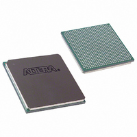
EP1S20F780I6N Altera, EP1S20F780I6N Datasheet - Page 414

EP1S20F780I6N
Manufacturer Part Number
EP1S20F780I6N
Description
IC STRATIX FPGA 20K LE 780-FBGA
Manufacturer
Altera
Series
Stratix®r
Specifications of EP1S20F780I6N
Number Of Logic Elements/cells
18460
Number Of Labs/clbs
1846
Total Ram Bits
1669248
Number Of I /o
586
Voltage - Supply
1.425 V ~ 1.575 V
Mounting Type
Surface Mount
Operating Temperature
-40°C ~ 100°C
Package / Case
780-FBGA
Family Name
Stratix
Number Of Logic Blocks/elements
18460
# I/os (max)
586
Frequency (max)
450.05MHz
Process Technology
0.13um (CMOS)
Operating Supply Voltage (typ)
1.5V
Logic Cells
18460
Ram Bits
1669248
Operating Supply Voltage (min)
1.425V
Operating Supply Voltage (max)
1.575V
Operating Temp Range
-40C to 100C
Operating Temperature Classification
Industrial
Mounting
Surface Mount
Pin Count
780
Package Type
FC-FBGA
Lead Free Status / RoHS Status
Lead free / RoHS Compliant
Number Of Gates
-
Lead Free Status / Rohs Status
Compliant
Available stocks
Company
Part Number
Manufacturer
Quantity
Price
Company:
Part Number:
EP1S20F780I6N
Manufacturer:
ALTERA
Quantity:
3 000
- Current page: 414 of 864
- Download datasheet (11Mb)
DDR Memory Support Overview
3–18
Stratix Device Handbook, Volume 2
To generate the correct phase shift, you must provide a clock signal of the
same frequency as the DQS signal to the DQS phase-shift circuitry. Any
of the CLK[15..12]p clock pins can feed the phase circuitry on the top
of the device (I/O banks 3 and 4) and any of the CLK[7..4]p clock pins
can feed the phase circuitry on the bottom of the device (I/O banks 7
and 8). Both the top and bottom phase-shift circuits need unique clock
pins for the reference clock. You cannot use any internal clock sources to
feed the phase-shift circuitry, but you can route internal clock sources
off-chip and then back into one of the allowable clock input pins.
DLL
The DQS phase-shift circuitry uses a DLL to dynamically measure the
clock period needed by the DQS pin (see
phase-shift circuitry then uses the clock period to generate the correct
phase shift. The DLL in the Stratix and Stratix GX devices DQS phase-
shift circuitry can operate between 100 and 200 MHz. The phase-shift
circuitry needs a maximum of 256 clock cycles to calculate the correct
phase shift. Data sent during these clock cycles may not be properly
captured.
1
Note to
(1)
Table 3–4. Quartus II Reported Number on the DQS Path to the
IOE
Speed Grade
These are reported by Quartus II version 4.0. Check the latest version of the
Quartus II software for the most current information.
Note (1)
Table
-8
You can still use the DQS phase-shift circuitry for DDR SDRAM
interfaces that are less than 100 MHz. The DQS signal is shifted
by about 2.5 ns. This shifted DQS signal is not in the center of the
DQ signals, but it is shifted enough to capture the correct data in
this low-frequency application.
3–4:
DQ2IOE
1.293
Figure
DQS2IOE
1.635
3–9). The DQS
Altera Corporation
Unit
ns
June 2006
Related parts for EP1S20F780I6N
Image
Part Number
Description
Manufacturer
Datasheet
Request
R

Part Number:
Description:
CYCLONE II STARTER KIT EP2C20N
Manufacturer:
Altera
Datasheet:

Part Number:
Description:
CPLD, EP610 Family, ECMOS Process, 300 Gates, 16 Macro Cells, 16 Reg., 16 User I/Os, 5V Supply, 35 Speed Grade, 24DIP
Manufacturer:
Altera Corporation
Datasheet:

Part Number:
Description:
CPLD, EP610 Family, ECMOS Process, 300 Gates, 16 Macro Cells, 16 Reg., 16 User I/Os, 5V Supply, 15 Speed Grade, 24DIP
Manufacturer:
Altera Corporation
Datasheet:

Part Number:
Description:
Manufacturer:
Altera Corporation
Datasheet:

Part Number:
Description:
CPLD, EP610 Family, ECMOS Process, 300 Gates, 16 Macro Cells, 16 Reg., 16 User I/Os, 5V Supply, 30 Speed Grade, 24DIP
Manufacturer:
Altera Corporation
Datasheet:

Part Number:
Description:
High-performance, low-power erasable programmable logic devices with 8 macrocells, 10ns
Manufacturer:
Altera Corporation
Datasheet:

Part Number:
Description:
High-performance, low-power erasable programmable logic devices with 8 macrocells, 7ns
Manufacturer:
Altera Corporation
Datasheet:

Part Number:
Description:
Classic EPLD
Manufacturer:
Altera Corporation
Datasheet:

Part Number:
Description:
High-performance, low-power erasable programmable logic devices with 8 macrocells, 10ns
Manufacturer:
Altera Corporation
Datasheet:

Part Number:
Description:
Manufacturer:
Altera Corporation
Datasheet:

Part Number:
Description:
Manufacturer:
Altera Corporation
Datasheet:

Part Number:
Description:
Manufacturer:
Altera Corporation
Datasheet:

Part Number:
Description:
CPLD, EP610 Family, ECMOS Process, 300 Gates, 16 Macro Cells, 16 Reg., 16 User I/Os, 5V Supply, 25 Speed Grade, 24DIP
Manufacturer:
Altera Corporation
Datasheet:


