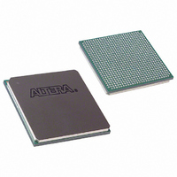
EP1S20F780I6N Altera, EP1S20F780I6N Datasheet - Page 388

EP1S20F780I6N
Manufacturer Part Number
EP1S20F780I6N
Description
IC STRATIX FPGA 20K LE 780-FBGA
Manufacturer
Altera
Series
Stratix®r
Specifications of EP1S20F780I6N
Number Of Logic Elements/cells
18460
Number Of Labs/clbs
1846
Total Ram Bits
1669248
Number Of I /o
586
Voltage - Supply
1.425 V ~ 1.575 V
Mounting Type
Surface Mount
Operating Temperature
-40°C ~ 100°C
Package / Case
780-FBGA
Family Name
Stratix
Number Of Logic Blocks/elements
18460
# I/os (max)
586
Frequency (max)
450.05MHz
Process Technology
0.13um (CMOS)
Operating Supply Voltage (typ)
1.5V
Logic Cells
18460
Ram Bits
1669248
Operating Supply Voltage (min)
1.425V
Operating Supply Voltage (max)
1.575V
Operating Temp Range
-40C to 100C
Operating Temperature Classification
Industrial
Mounting
Surface Mount
Pin Count
780
Package Type
FC-FBGA
Lead Free Status / RoHS Status
Lead free / RoHS Compliant
Number Of Gates
-
Lead Free Status / Rohs Status
Compliant
Available stocks
Company
Part Number
Manufacturer
Quantity
Price
Company:
Part Number:
EP1S20F780I6N
Manufacturer:
ALTERA
Quantity:
3 000
- Current page: 388 of 864
- Download datasheet (11Mb)
Clock Modes
Figure 2–11. Input/Output Clock Mode in Simple Dual-Port Mode
Notes to
(1)
(2)
(3)
(4)
2–20
Stratix Device Handbook, Volume 2
wraddress[ ]
address[ ]
byteena[ ]
outclken
wrclock
inclken
rdclock
data[ ]
The rden signal is not available in the M-RAM block. A M-RAM block in simple dual-port mode is always reading
out the data stored at the current read address location.
For more information on the MultiTrack™ interconnect, see the Stratix Device Family Data Sheet section of the Stratix
Device Handbook, Volume 1 or the Stratix GX Device Family Data Sheet section of the Stratix GX Device Handbook,
Volume 1.
All registers shown have asynchronous clear ports, except when using the M-RAM. M-RAM blocks have
asynchronous clear ports on their output registers only.
Violating the setup or hold time on the address registers could corrupt the memory contents. This applies to both
read and write operations.
wren
rden
Figure
8 LAB Row
Clocks
8
2–11:
All registers shown have asynchronous clear ports, except when using
the M-RAM. M-RAM blocks have asynchronous clear ports on their
output registers only.
D
ENA
D
ENA
D
ENA
D
ENA
D
ENA
D
ENA
Q
Q
Q
Q
Q
Q
Generator
Pulse
Write
Data In
Read Address
Byte Enable
Write Address
Read Enable
Write Enable
Notes
Memory Block
Data Out
1,024 ´ 4
2,048 ´ 2
4,096 ´ 1
256 ´ 16
(1), (2), (3),
512 ´ 8
D
ENA
(4)
Q
Altera Corporation
To MultiTrack
Interconnect
July 2005
Related parts for EP1S20F780I6N
Image
Part Number
Description
Manufacturer
Datasheet
Request
R

Part Number:
Description:
CYCLONE II STARTER KIT EP2C20N
Manufacturer:
Altera
Datasheet:

Part Number:
Description:
CPLD, EP610 Family, ECMOS Process, 300 Gates, 16 Macro Cells, 16 Reg., 16 User I/Os, 5V Supply, 35 Speed Grade, 24DIP
Manufacturer:
Altera Corporation
Datasheet:

Part Number:
Description:
CPLD, EP610 Family, ECMOS Process, 300 Gates, 16 Macro Cells, 16 Reg., 16 User I/Os, 5V Supply, 15 Speed Grade, 24DIP
Manufacturer:
Altera Corporation
Datasheet:

Part Number:
Description:
Manufacturer:
Altera Corporation
Datasheet:

Part Number:
Description:
CPLD, EP610 Family, ECMOS Process, 300 Gates, 16 Macro Cells, 16 Reg., 16 User I/Os, 5V Supply, 30 Speed Grade, 24DIP
Manufacturer:
Altera Corporation
Datasheet:

Part Number:
Description:
High-performance, low-power erasable programmable logic devices with 8 macrocells, 10ns
Manufacturer:
Altera Corporation
Datasheet:

Part Number:
Description:
High-performance, low-power erasable programmable logic devices with 8 macrocells, 7ns
Manufacturer:
Altera Corporation
Datasheet:

Part Number:
Description:
Classic EPLD
Manufacturer:
Altera Corporation
Datasheet:

Part Number:
Description:
High-performance, low-power erasable programmable logic devices with 8 macrocells, 10ns
Manufacturer:
Altera Corporation
Datasheet:

Part Number:
Description:
Manufacturer:
Altera Corporation
Datasheet:

Part Number:
Description:
Manufacturer:
Altera Corporation
Datasheet:

Part Number:
Description:
Manufacturer:
Altera Corporation
Datasheet:

Part Number:
Description:
CPLD, EP610 Family, ECMOS Process, 300 Gates, 16 Macro Cells, 16 Reg., 16 User I/Os, 5V Supply, 25 Speed Grade, 24DIP
Manufacturer:
Altera Corporation
Datasheet:


