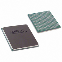
EP1S20F780I6N Altera, EP1S20F780I6N Datasheet - Page 404

EP1S20F780I6N
Manufacturer Part Number
EP1S20F780I6N
Description
IC STRATIX FPGA 20K LE 780-FBGA
Manufacturer
Altera
Series
Stratix®r
Specifications of EP1S20F780I6N
Number Of Logic Elements/cells
18460
Number Of Labs/clbs
1846
Total Ram Bits
1669248
Number Of I /o
586
Voltage - Supply
1.425 V ~ 1.575 V
Mounting Type
Surface Mount
Operating Temperature
-40°C ~ 100°C
Package / Case
780-FBGA
Family Name
Stratix
Number Of Logic Blocks/elements
18460
# I/os (max)
586
Frequency (max)
450.05MHz
Process Technology
0.13um (CMOS)
Operating Supply Voltage (typ)
1.5V
Logic Cells
18460
Ram Bits
1669248
Operating Supply Voltage (min)
1.425V
Operating Supply Voltage (max)
1.575V
Operating Temp Range
-40C to 100C
Operating Temperature Classification
Industrial
Mounting
Surface Mount
Pin Count
780
Package Type
FC-FBGA
Lead Free Status / RoHS Status
Lead free / RoHS Compliant
Number Of Gates
-
Lead Free Status / Rohs Status
Compliant
Available stocks
Company
Part Number
Manufacturer
Quantity
Price
Company:
Part Number:
EP1S20F780I6N
Manufacturer:
ALTERA
Quantity:
3 000
- Current page: 404 of 864
- Download datasheet (11Mb)
External Memory Standards
Figure 3–5. Data & Clock Relationship During a QDRII SRAM Read
Notes to
(1)
(2)
(3)
(4)
(5)
3–8
Stratix Device Handbook, Volume 2
Cn/Kn
CQn
CQ
C/K
Q
The timing parameter nomenclature is based on the Cypress QDRII SRAM data sheet for CY7C1313V18.
CO is the data clock-to-out time and t
t
t
t
CLZ
CQD
CQQO
Figure
and t
is the skew between CQn and data edges.
and t
CHZ
CQOH
3–5:
are bus turn-on and turn-off times respectively.
f
are skew between the C or Cn (or K or Kn in single-clock mode) and the CQ or CQn clocks.
clock mode, or K or Kn in single clock mode. The edge-aligned CQ and
CQn clocks accompany the read data for data capture in Stratix and
Stratix GX devices.
When writing to QDRII SRAM devices, data is generated by the write
clock, while the K clock is 90° shifted from the write clock, creating a
center-aligned arrangement.
Go to www.qdrsram.com for the QDR SRAM and QDRII SRAM
specifications. For more information on QDR and QDRII SRAM
interfaces in Stratix and Stratix GX devices, see AN 349: QDR SRAM
Controller Reference Design for Stratix & Stratix GX Devices.
ZBT SRAM
ZBT SRAM eliminate dead bus cycles when turning a bidirectional bus
around between reads and writes or between writes and reads. ZBT
allows for 100% bus utilization because ZBT SRAM can be read or written
on every clock cycle. Bus contention can occur when shifting from a write
cycle to a read cycle or vice versa with no idle cycles in between.
ZBT SRAM allows small amounts of bus contention. To avoid bus
contention, the output clock-to-low-impedance time (t
t
t
CCQO (5)
CLZ (3)
DOH
t
CO (2)
is the data output hold time between burst.
QA
t
QA + 1
DOH (2)
t
CQD (4)
t
t
CQOH (5)
CO (2)
Note (1)
QA + 2
QA + 3
t
t
CQD (4)
CHZ (3)
ZX
Altera Corporation
) must be greater
June 2006
Related parts for EP1S20F780I6N
Image
Part Number
Description
Manufacturer
Datasheet
Request
R

Part Number:
Description:
CYCLONE II STARTER KIT EP2C20N
Manufacturer:
Altera
Datasheet:

Part Number:
Description:
CPLD, EP610 Family, ECMOS Process, 300 Gates, 16 Macro Cells, 16 Reg., 16 User I/Os, 5V Supply, 35 Speed Grade, 24DIP
Manufacturer:
Altera Corporation
Datasheet:

Part Number:
Description:
CPLD, EP610 Family, ECMOS Process, 300 Gates, 16 Macro Cells, 16 Reg., 16 User I/Os, 5V Supply, 15 Speed Grade, 24DIP
Manufacturer:
Altera Corporation
Datasheet:

Part Number:
Description:
Manufacturer:
Altera Corporation
Datasheet:

Part Number:
Description:
CPLD, EP610 Family, ECMOS Process, 300 Gates, 16 Macro Cells, 16 Reg., 16 User I/Os, 5V Supply, 30 Speed Grade, 24DIP
Manufacturer:
Altera Corporation
Datasheet:

Part Number:
Description:
High-performance, low-power erasable programmable logic devices with 8 macrocells, 10ns
Manufacturer:
Altera Corporation
Datasheet:

Part Number:
Description:
High-performance, low-power erasable programmable logic devices with 8 macrocells, 7ns
Manufacturer:
Altera Corporation
Datasheet:

Part Number:
Description:
Classic EPLD
Manufacturer:
Altera Corporation
Datasheet:

Part Number:
Description:
High-performance, low-power erasable programmable logic devices with 8 macrocells, 10ns
Manufacturer:
Altera Corporation
Datasheet:

Part Number:
Description:
Manufacturer:
Altera Corporation
Datasheet:

Part Number:
Description:
Manufacturer:
Altera Corporation
Datasheet:

Part Number:
Description:
Manufacturer:
Altera Corporation
Datasheet:

Part Number:
Description:
CPLD, EP610 Family, ECMOS Process, 300 Gates, 16 Macro Cells, 16 Reg., 16 User I/Os, 5V Supply, 25 Speed Grade, 24DIP
Manufacturer:
Altera Corporation
Datasheet:


