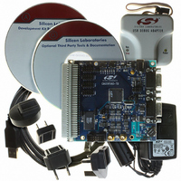
C8051F060DK Silicon Laboratories Inc, C8051F060DK Datasheet - Page 298

C8051F060DK
Manufacturer Part Number
C8051F060DK
Description
DEV KIT FOR F060/F062/F063
Manufacturer
Silicon Laboratories Inc
Type
MCUr
Datasheet
1.C8051F060-TB.pdf
(328 pages)
Specifications of C8051F060DK
Contents
Evaluation Board, Power Supply, USB Cables, Adapter and Documentation
Processor To Be Evaluated
C8051F06x
Interface Type
USB
Silicon Manufacturer
Silicon Labs
Core Architecture
8051
Silicon Core Number
C8051F060
Silicon Family Name
C8051F06x
Lead Free Status / RoHS Status
Contains lead / RoHS non-compliant
For Use With/related Products
C8051060, C8051F062 and C8051F063
Lead Free Status / Rohs Status
Lead free / RoHS Compliant
Other names
336-1214
Available stocks
Company
Part Number
Manufacturer
Quantity
Price
Company:
Part Number:
C8051F060DK
Manufacturer:
Silicon Labs
Quantity:
135
- Current page: 298 of 328
- Download datasheet (2Mb)
C8051F060/1/2/3/4/5/6/7
24.2.4. Toggle Output Mode
Timer 2, 3, and 4 have the capability to toggle the state of their respective output port pins (T2, T3, or T4)
to produce a 50% duty cycle waveform output. The port pin state will change upon the overflow or under-
flow of the respective timer (depending on whether the timer is counting up or down). The toggle frequency
is determined by the clock source of the timer and the values loaded into RCAPnH and RCAPnL. When
counting DOWN, the auto-reload value for the timer is 0xFFFF, and underflow will occur when the value in
the timer matches the value stored in RCAPnH:RCAPnL. When counting UP, the auto-reload value for the
timer is RCAPnH:RCAPnL, and overflow will occur when the value in the timer transitions from 0xFFFF to
the reload value.
To output a square wave, the timer is placed in reload mode (the Capture/Reload Select Bit in TMRnCN
and the Timer/Counter Select Bit in TMRnCN are cleared to ‘0’). The timer output is enabled by setting the
Timer Output Enable Bit in TMRnCF to ‘1’. The timer should be configured via the timer clock source and
reload/underflow values such that the timer overflow/underflows at 1/2 the desired output frequency. The
port pin assigned by the crossbar as the timer’s output pin should be configured as a digital output (see
Section “18. Port Input/Output” on page
the pin. A Read/Write of the Timer’s Toggle Output State Bit (TMRnCF.2) is used to read the state of the
toggle output, or to force a value of the output. This is useful when it is desired to start the toggle of a pin in
a known state, or to force the pin into a desired state when the toggle mode is halted.
298
Equation 24.1. Toggle Mode Square Wave Frequency
F
sq
203). Setting the timer’s Run Bit (TRn) to ‘1’ will start the toggle of
=
---------------------------------------------------- -
2
Rev. 1.2
65536 RCAPn
F
TCLK
–
Related parts for C8051F060DK
Image
Part Number
Description
Manufacturer
Datasheet
Request
R
Part Number:
Description:
SMD/C°/SINGLE-ENDED OUTPUT SILICON OSCILLATOR
Manufacturer:
Silicon Laboratories Inc
Part Number:
Description:
Manufacturer:
Silicon Laboratories Inc
Datasheet:
Part Number:
Description:
N/A N/A/SI4010 AES KEYFOB DEMO WITH LCD RX
Manufacturer:
Silicon Laboratories Inc
Datasheet:
Part Number:
Description:
N/A N/A/SI4010 SIMPLIFIED KEY FOB DEMO WITH LED RX
Manufacturer:
Silicon Laboratories Inc
Datasheet:
Part Number:
Description:
N/A/-40 TO 85 OC/EZLINK MODULE; F930/4432 HIGH BAND (REV E/B1)
Manufacturer:
Silicon Laboratories Inc
Part Number:
Description:
EZLink Module; F930/4432 Low Band (rev e/B1)
Manufacturer:
Silicon Laboratories Inc
Part Number:
Description:
I°/4460 10 DBM RADIO TEST CARD 434 MHZ
Manufacturer:
Silicon Laboratories Inc
Part Number:
Description:
I°/4461 14 DBM RADIO TEST CARD 868 MHZ
Manufacturer:
Silicon Laboratories Inc
Part Number:
Description:
I°/4463 20 DBM RFSWITCH RADIO TEST CARD 460 MHZ
Manufacturer:
Silicon Laboratories Inc
Part Number:
Description:
I°/4463 20 DBM RADIO TEST CARD 868 MHZ
Manufacturer:
Silicon Laboratories Inc
Part Number:
Description:
I°/4463 27 DBM RADIO TEST CARD 868 MHZ
Manufacturer:
Silicon Laboratories Inc
Part Number:
Description:
I°/4463 SKYWORKS 30 DBM RADIO TEST CARD 915 MHZ
Manufacturer:
Silicon Laboratories Inc
Part Number:
Description:
N/A N/A/-40 TO 85 OC/4463 RFMD 30 DBM RADIO TEST CARD 915 MHZ
Manufacturer:
Silicon Laboratories Inc
Part Number:
Description:
I°/4463 20 DBM RADIO TEST CARD 169 MHZ
Manufacturer:
Silicon Laboratories Inc


