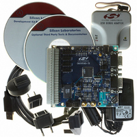
C8051F060DK Silicon Laboratories Inc, C8051F060DK Datasheet - Page 79

C8051F060DK
Manufacturer Part Number
C8051F060DK
Description
DEV KIT FOR F060/F062/F063
Manufacturer
Silicon Laboratories Inc
Type
MCUr
Datasheet
1.C8051F060-TB.pdf
(328 pages)
Specifications of C8051F060DK
Contents
Evaluation Board, Power Supply, USB Cables, Adapter and Documentation
Processor To Be Evaluated
C8051F06x
Interface Type
USB
Silicon Manufacturer
Silicon Labs
Core Architecture
8051
Silicon Core Number
C8051F060
Silicon Family Name
C8051F06x
Lead Free Status / RoHS Status
Contains lead / RoHS non-compliant
For Use With/related Products
C8051060, C8051F062 and C8051F063
Lead Free Status / Rohs Status
Lead free / RoHS Compliant
Other names
336-1214
Available stocks
Company
Part Number
Manufacturer
Quantity
Price
Company:
Part Number:
C8051F060DK
Manufacturer:
Silicon Labs
Quantity:
135
- Current page: 79 of 328
- Download datasheet (2Mb)
6.6.
The DMA contains multiple interrupt sources. Some of these can be individually enabled to generate inter-
rupts as necessary. The DMA Control Register (DMA0CN, Figure 6.4) and DMA Configuration Register
(DMA0CF, Figure 6.5) contain the enable bits and flags for the DMA interrupt sources. When an interrupt is
enabled and the interrupt condition occurs, a DMA interrupt will be generated (EIE2.7 is set to ‘1’).
The DMA flags that can generate a DMA0 interrupt are:
6.7.
The data paths from the ADCs to XRAM are double-buffered when using the DMA interface. When a con-
version is completed by the ADC, it first enters the ADCs data register. If the DMA’s data buffer is empty,
the conversion results will immediately be written into the DMA’s internal data buffer for that ADC. Data in
the DMA’s internal data buffer is written to XRAM at the first available opportunity (see
Addressing and Setup” on page
the DMA’s data buffer until data in the buffer has been written to XRAM. When a conversion is completed
and the DMA’s data buffer is not empty, an overflow warning flag is generated. If a second conversion data
word becomes available before the DMA’s data buffer is written to XRAM, the data in the ADC’s data regis-
ters is over-written with the new data word, and a data overflow error flag is generated.
Interrupt Sources
1. DMA Operations Complete (DMA0CN.6, DMA0INT) occurs when all DMA operations have
2. ADC1 Data Overflow Error (DMA0CN.4, DMA0DE1) occurs when the DMA interface cannot
3. ADC0 Data Overflow Error (DMA0CN.3, DMA0DE0) occurs when the DMA interface cannot
4. ADC1 Data Overflow Warning (DMA0CN.1, DMA0DO1) occurs when data from ADC0
5. ADC0 Data Overflow Warning (DMA0CN.0, DMA0DO0) occurs when data from ADC1
6. Repeat Counter Overflow (DMA0CF.2, DMA0CI) occurs when the Repeat Counter reaches
7. End Of Operation (DMA0CF.0, DMA0EO) occurs when an End Of Operation instruction is
Data Buffer Overflow Warnings and Errors
been completed, and the DMA interface is idle.
access XRAM for two conversion cycles of ADC1. This flag indicates that at least one conver-
sion result from ADC1 has been discarded.
access XRAM for two conversion cycles of ADC0. This flag indicates that at least one conver-
sion result from ADC0 has been discarded.
becomes available and the DMA has not yet written the previous results to XRAM. This inter-
rupt source can be enabled and disabled with the Data Overflow Warning Enable bit
(DMA0CN.2, DMA0DOE).
becomes available and the DMA has not yet written the previous results to XRAM. This inter-
rupt source can be enabled and disabled with the Data Overflow Warning Enable bit
(DMA0CN.2, DMA0DOE).
the Repeat Counter Limit. This interrupt source can be enabled and disabled with the Repeat
Counter Overflow Interrupt Enable bit (DMA0CF.3, DMA0CIE).
reached in the Instruction Buffer. This interrupt source can be enabled and disabled with the
End Of Operation Interrupt Enable bit (DMA0CF.1, DMA0EOE).
76). Conversion results from the ADC’s data registers are not copied into
Rev. 1.2
C8051F060/1/2/3/4/5/6/7
Section “6.3. XRAM
79
Related parts for C8051F060DK
Image
Part Number
Description
Manufacturer
Datasheet
Request
R
Part Number:
Description:
SMD/C°/SINGLE-ENDED OUTPUT SILICON OSCILLATOR
Manufacturer:
Silicon Laboratories Inc
Part Number:
Description:
Manufacturer:
Silicon Laboratories Inc
Datasheet:
Part Number:
Description:
N/A N/A/SI4010 AES KEYFOB DEMO WITH LCD RX
Manufacturer:
Silicon Laboratories Inc
Datasheet:
Part Number:
Description:
N/A N/A/SI4010 SIMPLIFIED KEY FOB DEMO WITH LED RX
Manufacturer:
Silicon Laboratories Inc
Datasheet:
Part Number:
Description:
N/A/-40 TO 85 OC/EZLINK MODULE; F930/4432 HIGH BAND (REV E/B1)
Manufacturer:
Silicon Laboratories Inc
Part Number:
Description:
EZLink Module; F930/4432 Low Band (rev e/B1)
Manufacturer:
Silicon Laboratories Inc
Part Number:
Description:
I°/4460 10 DBM RADIO TEST CARD 434 MHZ
Manufacturer:
Silicon Laboratories Inc
Part Number:
Description:
I°/4461 14 DBM RADIO TEST CARD 868 MHZ
Manufacturer:
Silicon Laboratories Inc
Part Number:
Description:
I°/4463 20 DBM RFSWITCH RADIO TEST CARD 460 MHZ
Manufacturer:
Silicon Laboratories Inc
Part Number:
Description:
I°/4463 20 DBM RADIO TEST CARD 868 MHZ
Manufacturer:
Silicon Laboratories Inc
Part Number:
Description:
I°/4463 27 DBM RADIO TEST CARD 868 MHZ
Manufacturer:
Silicon Laboratories Inc
Part Number:
Description:
I°/4463 SKYWORKS 30 DBM RADIO TEST CARD 915 MHZ
Manufacturer:
Silicon Laboratories Inc
Part Number:
Description:
N/A N/A/-40 TO 85 OC/4463 RFMD 30 DBM RADIO TEST CARD 915 MHZ
Manufacturer:
Silicon Laboratories Inc
Part Number:
Description:
I°/4463 20 DBM RADIO TEST CARD 169 MHZ
Manufacturer:
Silicon Laboratories Inc


