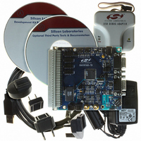
C8051F060DK Silicon Laboratories Inc, C8051F060DK Datasheet - Page 76

C8051F060DK
Manufacturer Part Number
C8051F060DK
Description
DEV KIT FOR F060/F062/F063
Manufacturer
Silicon Laboratories Inc
Type
MCUr
Datasheet
1.C8051F060-TB.pdf
(328 pages)
Specifications of C8051F060DK
Contents
Evaluation Board, Power Supply, USB Cables, Adapter and Documentation
Processor To Be Evaluated
C8051F06x
Interface Type
USB
Silicon Manufacturer
Silicon Labs
Core Architecture
8051
Silicon Core Number
C8051F060
Silicon Family Name
C8051F06x
Lead Free Status / RoHS Status
Contains lead / RoHS non-compliant
For Use With/related Products
C8051060, C8051F062 and C8051F063
Lead Free Status / Rohs Status
Lead free / RoHS Compliant
Other names
336-1214
Available stocks
Company
Part Number
Manufacturer
Quantity
Price
Company:
Part Number:
C8051F060DK
Manufacturer:
Silicon Labs
Quantity:
135
- Current page: 76 of 328
- Download datasheet (2Mb)
C8051F060/1/2/3/4/5/6/7
6.2.
DMA instructions can request single-ended data from both ADC0 and ADC1, as well as the differential
combination of the two ADC inputs. The instruction format is identical to the DMA0IDT register, shown in
Figure 6.7. Depending on which bits are set to ‘1’ in the instruction word, either 2 or 4 bytes of data will be
written to XRAM for each DMA instruction cycle (excluding End-Of-Operation instructions). Table 6.1
details all of the valid DMA instructions. Instructions not listed in the table are not valid DMA instructions,
and should not be used. Note that the ADCs can be independently controlled by the microcontroller when
their outputs are not requested by the DMA.
6.3.
The DMA Interface can be configured to access either on-chip or off-chip XRAM. Any writes to on-chip
XRAM by the DMA Control Logic occur when the processor core is not accessing the on-chip XRAM. This
ensures that the DMA will not interfere with processor instruction timing.
Off-chip XRAM access (only available on the C8051F060/2/4/6) is controlled by the DMA0HLT bit in
DMA0CF (DMA Configuration Register, Figure 6.5). The DMA will have full access to off-chip XRAM when
this bit is ‘0’, and the processor core will have full access to off-chip XRAM when this bit is ‘1’. The
DMA0HLT bit should be controlled in software when both the processor core and the DMA Interface
require access to off-chip XRAM data space. Before setting DMA0HLT to ‘1’, the software should check the
DMA0XBY bit to ensure that the DMA is not currently accessing off-chip XRAM. The processor core can-
not access off-chip XRAM while DMA0HLT is ‘0’. The processor will continue as though it was able to per-
form the desired memory access, but the data will not be written to or read from off-chip XRAM. When the
processor core is finished accessing off-chip XRAM, DMA0HLT should be set back to ‘0’in software to
return control to the DMA Interface. The DMA Control Logic will wait until DMA0HLT is ‘0’ before writing
data to off-chip XRAM. If new data becomes available to the DMA Interface before the previous data has
been written, an overflow condition will occur, and the new data word may be lost.
The Data Address Pointer Registers (DMA0DSH and DMA0DSL) contain the 16-bit XRAM address loca-
tion where the DMA interface will write data. When the DMA is initially enabled, the DMA Data Address
76
Instruction
Word
00000000b End-Of-Operation
10000000b End-Of-Operation with Continuous Conversion
x0010000b Retrieve ADC0 Data
x0100000b Retrieve ADC1 Data
x0110000b Retrieve ADC0 and ADC1 Data
x10x0000b Retrieve Differential Data
x11x0000b
DMA0 Instruction Format
XRAM Addressing and Setup
Description
Retrieve Differential and ADC1 Data
Table 6.1. DMA0 Instruction Set
Rev. 1.2
to XRAM (2 bytes)
First Data Written
(differential result
(differential result
from both ADCs)
from both ADCs)
ADC0H:ADC0L
ADC1H:ADC1L
ADC0H:ADC0L
ADC0H:ADC0L
ADC0H:ADC0L
none
none
Written to XRAM
ADC1H:ADC1L
ADC1H:ADC1L
Second Data
(2 bytes)
none
none
none
none
none
Related parts for C8051F060DK
Image
Part Number
Description
Manufacturer
Datasheet
Request
R
Part Number:
Description:
SMD/C°/SINGLE-ENDED OUTPUT SILICON OSCILLATOR
Manufacturer:
Silicon Laboratories Inc
Part Number:
Description:
Manufacturer:
Silicon Laboratories Inc
Datasheet:
Part Number:
Description:
N/A N/A/SI4010 AES KEYFOB DEMO WITH LCD RX
Manufacturer:
Silicon Laboratories Inc
Datasheet:
Part Number:
Description:
N/A N/A/SI4010 SIMPLIFIED KEY FOB DEMO WITH LED RX
Manufacturer:
Silicon Laboratories Inc
Datasheet:
Part Number:
Description:
N/A/-40 TO 85 OC/EZLINK MODULE; F930/4432 HIGH BAND (REV E/B1)
Manufacturer:
Silicon Laboratories Inc
Part Number:
Description:
EZLink Module; F930/4432 Low Band (rev e/B1)
Manufacturer:
Silicon Laboratories Inc
Part Number:
Description:
I°/4460 10 DBM RADIO TEST CARD 434 MHZ
Manufacturer:
Silicon Laboratories Inc
Part Number:
Description:
I°/4461 14 DBM RADIO TEST CARD 868 MHZ
Manufacturer:
Silicon Laboratories Inc
Part Number:
Description:
I°/4463 20 DBM RFSWITCH RADIO TEST CARD 460 MHZ
Manufacturer:
Silicon Laboratories Inc
Part Number:
Description:
I°/4463 20 DBM RADIO TEST CARD 868 MHZ
Manufacturer:
Silicon Laboratories Inc
Part Number:
Description:
I°/4463 27 DBM RADIO TEST CARD 868 MHZ
Manufacturer:
Silicon Laboratories Inc
Part Number:
Description:
I°/4463 SKYWORKS 30 DBM RADIO TEST CARD 915 MHZ
Manufacturer:
Silicon Laboratories Inc
Part Number:
Description:
N/A N/A/-40 TO 85 OC/4463 RFMD 30 DBM RADIO TEST CARD 915 MHZ
Manufacturer:
Silicon Laboratories Inc
Part Number:
Description:
I°/4463 20 DBM RADIO TEST CARD 169 MHZ
Manufacturer:
Silicon Laboratories Inc


