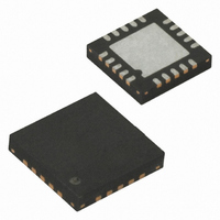
ATTINY43U-MU Atmel, ATTINY43U-MU Datasheet - Page 100

ATTINY43U-MU
Manufacturer Part Number
ATTINY43U-MU
Description
MCU AVR 4K FLASH 8MHZ 20-QFN
Manufacturer
Atmel
Series
AVR® ATtinyr
Specifications of ATTINY43U-MU
Core Processor
AVR
Core Size
8-Bit
Speed
8MHz
Connectivity
USI
Peripherals
Brown-out Detect/Reset, POR, PWM, Temp Sensor, WDT
Number Of I /o
16
Program Memory Size
4KB (2K x 16)
Program Memory Type
FLASH
Eeprom Size
64 x 8
Ram Size
256 x 8
Voltage - Supply (vcc/vdd)
1.8 V ~ 5.5 V
Data Converters
A/D 4x10b
Oscillator Type
Internal
Operating Temperature
-40°C ~ 85°C
Package / Case
20-MLF®, QFN
Processor Series
ATTINY4x
Core
AVR8
Data Bus Width
8 bit
Data Ram Size
256 B
Interface Type
SPI
Maximum Clock Frequency
8 MHz
Number Of Programmable I/os
16
Number Of Timers
2
Maximum Operating Temperature
+ 85 C
Mounting Style
SMD/SMT
3rd Party Development Tools
EWAVR, EWAVR-BL
Development Tools By Supplier
ATAVRDRAGON, ATSTK500, ATSTK600, ATAVRISP2, ATAVRONEKIT
Minimum Operating Temperature
- 40 C
On-chip Adc
10 bit, 4 Channel
For Use With
ATSTK600-TINYX3U - STK600 SOCKET/ADAPTER TINYX3U
Lead Free Status / RoHS Status
Lead free / RoHS Compliant
- Current page: 100 of 182
- Download datasheet (4Mb)
14. USI – Universal Serial Interface
14.1
14.2
100
Features
Overview
ATtiny43U
•
•
•
•
•
•
The Universal Serial Interface (USI), provides the basic hardware resources needed for serial
communication. Combined with a minimum of control software, the USI allows significantly
higher transfer rates and uses less code space than solutions based on software only. Interrupts
are included to minimize the processor load.
A simplified block diagram of the USI is shown in
of I/O pins, refer to
bits and I/O pins, are shown in bold. The device-specific I/O Register and bit locations are listed
in the
Figure 14-1. Universal Serial Interface, Block Diagram
The 8-bit USI Data Register (USIDR) contains the incoming and outgoing data. It is directly
accessible via the data bus but a copy of the contents is also placed in the USI Buffer Register
(USIBR) where it can be retrieved later. If reading the USI Data Register directly, the register
must be read as quickly as possible to ensure that no data is lost.
The most significant bit of the USI Data Register is connected to one of two output pins (depend-
ing on the mode configuration, see
between the output of the USI Data Register and the output pin, which delays the change of data
Two-wire Synchronous Data Transfer (Master or Slave)
Three-wire Synchronous Data Transfer (Master or Slave)
Data Received Interrupt
Wakeup from Idle Mode
In Two-wire Mode: Wake-up from All Sleep Modes, Including Power-down Mode
Two-wire Start Condition Detector with Interrupt Capability
“Register Descriptions” on page
USIDR
USIDB
USISR
USICR
2
“Pinout of ATtiny43U” on page
4-bit Counter
Table 14-1 on page
107.
3
2
1
0
3
2
1
0
D Q
LE
[1]
Figure 14-1 on page
2. CPU accessible I/O Registers, including I/O
TIM0 COMP
0
1
108). There is a transparent latch
Two-wire Clock
Control Unit
100. For actual placement
CLOCK
HOLD
DO
DI/SDA
USCK/SCL
8048B–AVR–03/09
(Output only)
(Input/Open Drain)
(Input/Open Drain)
Related parts for ATTINY43U-MU
Image
Part Number
Description
Manufacturer
Datasheet
Request
R

Part Number:
Description:
Manufacturer:
Atmel Corporation
Datasheet:

Part Number:
Description:
Microcontrollers (MCU) 512B FL 32B SRAM TIMER ATTINY4 12MHz
Manufacturer:
Atmel

Part Number:
Description:
IC MCU AVR 512B FLASH SOT-23-6
Manufacturer:
Atmel
Datasheet:

Part Number:
Description:
IC MCU AVR 512B FLASH SOT-23-6
Manufacturer:
Atmel
Datasheet:

Part Number:
Description:
DEV KIT FOR AVR/AVR32
Manufacturer:
Atmel
Datasheet:

Part Number:
Description:
INTERVAL AND WIPE/WASH WIPER CONTROL IC WITH DELAY
Manufacturer:
ATMEL Corporation
Datasheet:

Part Number:
Description:
Low-Voltage Voice-Switched IC for Hands-Free Operation
Manufacturer:
ATMEL Corporation
Datasheet:

Part Number:
Description:
MONOLITHIC INTEGRATED FEATUREPHONE CIRCUIT
Manufacturer:
ATMEL Corporation
Datasheet:

Part Number:
Description:
AM-FM Receiver IC U4255BM-M
Manufacturer:
ATMEL Corporation
Datasheet:

Part Number:
Description:
Monolithic Integrated Feature Phone Circuit
Manufacturer:
ATMEL Corporation
Datasheet:

Part Number:
Description:
Multistandard Video-IF and Quasi Parallel Sound Processing
Manufacturer:
ATMEL Corporation
Datasheet:


