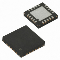
ATTINY43U-MU Atmel, ATTINY43U-MU Datasheet - Page 106

ATTINY43U-MU
Manufacturer Part Number
ATTINY43U-MU
Description
MCU AVR 4K FLASH 8MHZ 20-QFN
Manufacturer
Atmel
Series
AVR® ATtinyr
Specifications of ATTINY43U-MU
Core Processor
AVR
Core Size
8-Bit
Speed
8MHz
Connectivity
USI
Peripherals
Brown-out Detect/Reset, POR, PWM, Temp Sensor, WDT
Number Of I /o
16
Program Memory Size
4KB (2K x 16)
Program Memory Type
FLASH
Eeprom Size
64 x 8
Ram Size
256 x 8
Voltage - Supply (vcc/vdd)
1.8 V ~ 5.5 V
Data Converters
A/D 4x10b
Oscillator Type
Internal
Operating Temperature
-40°C ~ 85°C
Package / Case
20-MLF®, QFN
Processor Series
ATTINY4x
Core
AVR8
Data Bus Width
8 bit
Data Ram Size
256 B
Interface Type
SPI
Maximum Clock Frequency
8 MHz
Number Of Programmable I/os
16
Number Of Timers
2
Maximum Operating Temperature
+ 85 C
Mounting Style
SMD/SMT
3rd Party Development Tools
EWAVR, EWAVR-BL
Development Tools By Supplier
ATAVRDRAGON, ATSTK500, ATSTK600, ATAVRISP2, ATAVRONEKIT
Minimum Operating Temperature
- 40 C
On-chip Adc
10 bit, 4 Channel
For Use With
ATSTK600-TINYX3U - STK600 SOCKET/ADAPTER TINYX3U
Lead Free Status / RoHS Status
Lead free / RoHS Compliant
- Current page: 106 of 182
- Download datasheet (4Mb)
14.3.5
106
ATtiny43U
Start Condition Detector
If the slave is not able to receive more data it does not acknowledge the data byte it has last
received. When the master does a read operation it must terminate the operation by forcing the
acknowledge bit low after the last byte transmitted.
The start condition detector is shown in
to 300 ns) to ensure valid sampling of the SCL line. The start condition detector is only enabled
in two-wire mode.
Figure 14-6. Start Condition Detector, Logic Diagram
The start condition detector works asynchronously and can therefore wake up the processor
from power-down sleep mode. However, the protocol used might have restrictions on the SCL
hold time. Therefore, when using this feature the oscillator start-up time (set by CKSEL fuses,
see
of the USISIF bit on
2. In addition, the start detector will hold the SCL line low after the master has forced a
3. The master set the first bit to be transferred and releases the SCL line (C). The slave
4. After eight bits containing slave address and data direction (read or write) have been
5. When the slave is addressed, it holds the SDA line low during the acknowledgment
6. Multiple bytes can now be transmitted, all in same direction, until a stop condition is
“Clock Sources” on page
detects the start condition and sets the USISIF Flag. The flag can generate an interrupt
if necessary.
negative edge on this line (B). This allows the slave to wake up from sleep or complete
other tasks before setting up the USI Data Register to receive the address. This is done
by clearing the start condition flag and resetting the counter.
samples the data and shifts it into the USI Data Register at the positive edge of the SCL
clock.
transferred, the slave counter overflows and the SCL line is forced low (D). If the slave
is not the one the master has addressed, it releases the SCL line and waits for a new
start condition.
cycle before holding the SCL line low again (i.e., the USI Counter Register must be set
to 14 before releasing SCL at (D)). Depending on the R/W bit the master or slave
enables its output. If the bit is set, a master read operation is in progress (i.e., the slave
drives the SDA line) The slave can hold the SCL line low after the acknowledge (E).
given by the master (F), or a new start condition is given.
Write( USISIF)
page 112
SDA
SCL
24) must also be taken into consideration. Refer to the description
for further details.
Figure
14-6. The SDA line is delayed (in the range of 50
D Q
CLR
D Q
CLR
USISIF
CLOCK
HOLD
8048B–AVR–03/09
Related parts for ATTINY43U-MU
Image
Part Number
Description
Manufacturer
Datasheet
Request
R

Part Number:
Description:
Manufacturer:
Atmel Corporation
Datasheet:

Part Number:
Description:
Microcontrollers (MCU) 512B FL 32B SRAM TIMER ATTINY4 12MHz
Manufacturer:
Atmel

Part Number:
Description:
IC MCU AVR 512B FLASH SOT-23-6
Manufacturer:
Atmel
Datasheet:

Part Number:
Description:
IC MCU AVR 512B FLASH SOT-23-6
Manufacturer:
Atmel
Datasheet:

Part Number:
Description:
DEV KIT FOR AVR/AVR32
Manufacturer:
Atmel
Datasheet:

Part Number:
Description:
INTERVAL AND WIPE/WASH WIPER CONTROL IC WITH DELAY
Manufacturer:
ATMEL Corporation
Datasheet:

Part Number:
Description:
Low-Voltage Voice-Switched IC for Hands-Free Operation
Manufacturer:
ATMEL Corporation
Datasheet:

Part Number:
Description:
MONOLITHIC INTEGRATED FEATUREPHONE CIRCUIT
Manufacturer:
ATMEL Corporation
Datasheet:

Part Number:
Description:
AM-FM Receiver IC U4255BM-M
Manufacturer:
ATMEL Corporation
Datasheet:

Part Number:
Description:
Monolithic Integrated Feature Phone Circuit
Manufacturer:
ATMEL Corporation
Datasheet:

Part Number:
Description:
Multistandard Video-IF and Quasi Parallel Sound Processing
Manufacturer:
ATMEL Corporation
Datasheet:


