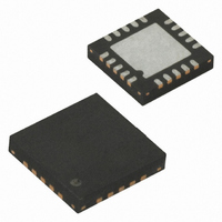
ATTINY43U-MU Atmel, ATTINY43U-MU Datasheet - Page 94

ATTINY43U-MU
Manufacturer Part Number
ATTINY43U-MU
Description
MCU AVR 4K FLASH 8MHZ 20-QFN
Manufacturer
Atmel
Series
AVR® ATtinyr
Specifications of ATTINY43U-MU
Core Processor
AVR
Core Size
8-Bit
Speed
8MHz
Connectivity
USI
Peripherals
Brown-out Detect/Reset, POR, PWM, Temp Sensor, WDT
Number Of I /o
16
Program Memory Size
4KB (2K x 16)
Program Memory Type
FLASH
Eeprom Size
64 x 8
Ram Size
256 x 8
Voltage - Supply (vcc/vdd)
1.8 V ~ 5.5 V
Data Converters
A/D 4x10b
Oscillator Type
Internal
Operating Temperature
-40°C ~ 85°C
Package / Case
20-MLF®, QFN
Processor Series
ATTINY4x
Core
AVR8
Data Bus Width
8 bit
Data Ram Size
256 B
Interface Type
SPI
Maximum Clock Frequency
8 MHz
Number Of Programmable I/os
16
Number Of Timers
2
Maximum Operating Temperature
+ 85 C
Mounting Style
SMD/SMT
3rd Party Development Tools
EWAVR, EWAVR-BL
Development Tools By Supplier
ATAVRDRAGON, ATSTK500, ATSTK600, ATAVRISP2, ATAVRONEKIT
Minimum Operating Temperature
- 40 C
On-chip Adc
10 bit, 4 Channel
For Use With
ATSTK600-TINYX3U - STK600 SOCKET/ADAPTER TINYX3U
Lead Free Status / RoHS Status
Lead free / RoHS Compliant
- Current page: 94 of 182
- Download datasheet (4Mb)
12.9.5
94
ATtiny43U
TCNT0 – Timer/Counter Register
However, for ensuring compatibility with future devices, this bit must be set to zero when
TCCR0B is written when operating in PWM mode. When writing a logical one to the FOCnB bit,
an immediate Compare Match is forced on the Waveform Generation unit. The OCnB output is
changed according to its COMnB1:0 bits setting. Note that the FOCnB bit is implemented as a
strobe. Therefore it is the value present in the COMnB1:0 bits that determines the effect of the
forced compare.
A FOCnB strobe will not generate any interrupt, nor will it clear the timer in CTC mode using
OCRnB as TOP.
The FOCnB bit is always read as zero.
• Bits 5, 4 – Res: Reserved Bits
These bits are reserved and will always read zero.
• Bit 3 – WGMn2: Waveform Generation Mode
See the description in the
• Bits 2:0 – CSn[2:0]: Clock Select
The three Clock Select bits select the clock source to be used by the Timer/Counter.
Table 12-9.
If external pin modes are used for the Timer/Countern, transitions on the Tn pin will clock the
counter even if the pin is configured as an output. This feature allows software control of the
counting.
Bit
0x32 (0x52)
Read/Write
Initial Value
CSn2
0
0
0
0
1
1
1
1
CSn1
0
0
1
1
0
0
1
1
Clock Select Bit Description
R/W
7
0
CSn0
0
1
0
1
0
1
0
1
R/W
“Register Description” on page
6
0
Description
No clock source (Timer/Counter stopped)
clk
clk
clk
clk
clk
External clock source on Tn pin. Clock on falling edge.
External clock source on Tn pin. Clock on rising edge.
I/O
I/O
I/O
I/O
I/O
/(No prescaling)
/8 (From prescaler)
/64 (From prescaler)
/256 (From prescaler)
/1024 (From prescaler)
R/W
5
0
R/W
4
0
TCNT0[7:0]
R/W
3
0
90.
R/W
2
0
R/W
1
0
R/W
0
0
8048B–AVR–03/09
TCNT0
Related parts for ATTINY43U-MU
Image
Part Number
Description
Manufacturer
Datasheet
Request
R

Part Number:
Description:
Manufacturer:
Atmel Corporation
Datasheet:

Part Number:
Description:
Microcontrollers (MCU) 512B FL 32B SRAM TIMER ATTINY4 12MHz
Manufacturer:
Atmel

Part Number:
Description:
IC MCU AVR 512B FLASH SOT-23-6
Manufacturer:
Atmel
Datasheet:

Part Number:
Description:
IC MCU AVR 512B FLASH SOT-23-6
Manufacturer:
Atmel
Datasheet:

Part Number:
Description:
DEV KIT FOR AVR/AVR32
Manufacturer:
Atmel
Datasheet:

Part Number:
Description:
INTERVAL AND WIPE/WASH WIPER CONTROL IC WITH DELAY
Manufacturer:
ATMEL Corporation
Datasheet:

Part Number:
Description:
Low-Voltage Voice-Switched IC for Hands-Free Operation
Manufacturer:
ATMEL Corporation
Datasheet:

Part Number:
Description:
MONOLITHIC INTEGRATED FEATUREPHONE CIRCUIT
Manufacturer:
ATMEL Corporation
Datasheet:

Part Number:
Description:
AM-FM Receiver IC U4255BM-M
Manufacturer:
ATMEL Corporation
Datasheet:

Part Number:
Description:
Monolithic Integrated Feature Phone Circuit
Manufacturer:
ATMEL Corporation
Datasheet:

Part Number:
Description:
Multistandard Video-IF and Quasi Parallel Sound Processing
Manufacturer:
ATMEL Corporation
Datasheet:


