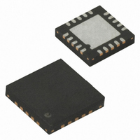
ATTINY43U-MU Atmel, ATTINY43U-MU Datasheet - Page 15

ATTINY43U-MU
Manufacturer Part Number
ATTINY43U-MU
Description
MCU AVR 4K FLASH 8MHZ 20-QFN
Manufacturer
Atmel
Series
AVR® ATtinyr
Specifications of ATTINY43U-MU
Core Processor
AVR
Core Size
8-Bit
Speed
8MHz
Connectivity
USI
Peripherals
Brown-out Detect/Reset, POR, PWM, Temp Sensor, WDT
Number Of I /o
16
Program Memory Size
4KB (2K x 16)
Program Memory Type
FLASH
Eeprom Size
64 x 8
Ram Size
256 x 8
Voltage - Supply (vcc/vdd)
1.8 V ~ 5.5 V
Data Converters
A/D 4x10b
Oscillator Type
Internal
Operating Temperature
-40°C ~ 85°C
Package / Case
20-MLF®, QFN
Processor Series
ATTINY4x
Core
AVR8
Data Bus Width
8 bit
Data Ram Size
256 B
Interface Type
SPI
Maximum Clock Frequency
8 MHz
Number Of Programmable I/os
16
Number Of Timers
2
Maximum Operating Temperature
+ 85 C
Mounting Style
SMD/SMT
3rd Party Development Tools
EWAVR, EWAVR-BL
Development Tools By Supplier
ATAVRDRAGON, ATSTK500, ATSTK600, ATAVRISP2, ATAVRONEKIT
Minimum Operating Temperature
- 40 C
On-chip Adc
10 bit, 4 Channel
For Use With
ATSTK600-TINYX3U - STK600 SOCKET/ADAPTER TINYX3U
Lead Free Status / RoHS Status
Lead free / RoHS Compliant
- Current page: 15 of 182
- Download datasheet (4Mb)
5. Memories
5.1
5.2
5.3
8048B–AVR–03/09
Overview
In-System Re-programmable Flash Program Memory
SRAM Data Memory
This section describes the different memories in ATtiny43U. The AVR architecture has two main
memory spaces, the Data memory and the Program memory space. In addition, the ATtiny43U
features an EEPROM Memory for data storage. All three memory spaces are linear and regular.
The ATtiny43U contains 4K byte On-chip In-System Reprogrammable Flash memory for pro-
gram storage. Since all AVR instructions are 16 or 32 bits wide, the Flash is organized as 2048 x
16.
The Flash memory has an endurance of at least 10,000 write/erase cycles. The ATtiny43U Pro-
gram Counter (PC) is 11 bits wide, thus addressing the 2048 Program memory locations.
“Memory Programming” on page 139
Constant tables can be allocated within the entire Program memory address space (see the
LPM – Load Program memory instruction description).
Timing diagrams for instruction fetch and execution are presented in
ing” on page
Figure 5-1.
Figure 5-2 on page 16
The low Data memory locations address both the Register File, the I/O memory and the internal
data SRAM, as follows:
The five different addressing modes for the Data memory cover: Direct, Indirect with Displace-
ment, Indirect, Indirect with Pre-decrement, and Indirect with Post-increment. In the Register
File, registers R26 to R31 feature the indirect addressing pointer registers.
• The first 32 locations address the Register File
• The next 64 locations address the standard I/O memory
• The last 256 locations address the internal data SRAM
12.
Program Memory Map
shows how the ATtiny43U SRAM Memory is organized.
Program Memory
contains a detailed description on Flash data downloading.
0x07FF
0x0000
“Instruction Execution Tim-
15
Related parts for ATTINY43U-MU
Image
Part Number
Description
Manufacturer
Datasheet
Request
R

Part Number:
Description:
Manufacturer:
Atmel Corporation
Datasheet:

Part Number:
Description:
Microcontrollers (MCU) 512B FL 32B SRAM TIMER ATTINY4 12MHz
Manufacturer:
Atmel

Part Number:
Description:
IC MCU AVR 512B FLASH SOT-23-6
Manufacturer:
Atmel
Datasheet:

Part Number:
Description:
IC MCU AVR 512B FLASH SOT-23-6
Manufacturer:
Atmel
Datasheet:

Part Number:
Description:
DEV KIT FOR AVR/AVR32
Manufacturer:
Atmel
Datasheet:

Part Number:
Description:
INTERVAL AND WIPE/WASH WIPER CONTROL IC WITH DELAY
Manufacturer:
ATMEL Corporation
Datasheet:

Part Number:
Description:
Low-Voltage Voice-Switched IC for Hands-Free Operation
Manufacturer:
ATMEL Corporation
Datasheet:

Part Number:
Description:
MONOLITHIC INTEGRATED FEATUREPHONE CIRCUIT
Manufacturer:
ATMEL Corporation
Datasheet:

Part Number:
Description:
AM-FM Receiver IC U4255BM-M
Manufacturer:
ATMEL Corporation
Datasheet:

Part Number:
Description:
Monolithic Integrated Feature Phone Circuit
Manufacturer:
ATMEL Corporation
Datasheet:

Part Number:
Description:
Multistandard Video-IF and Quasi Parallel Sound Processing
Manufacturer:
ATMEL Corporation
Datasheet:


