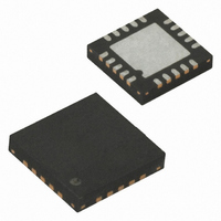
ATTINY43U-MU Atmel, ATTINY43U-MU Datasheet - Page 145

ATTINY43U-MU
Manufacturer Part Number
ATTINY43U-MU
Description
MCU AVR 4K FLASH 8MHZ 20-QFN
Manufacturer
Atmel
Series
AVR® ATtinyr
Specifications of ATTINY43U-MU
Core Processor
AVR
Core Size
8-Bit
Speed
8MHz
Connectivity
USI
Peripherals
Brown-out Detect/Reset, POR, PWM, Temp Sensor, WDT
Number Of I /o
16
Program Memory Size
4KB (2K x 16)
Program Memory Type
FLASH
Eeprom Size
64 x 8
Ram Size
256 x 8
Voltage - Supply (vcc/vdd)
1.8 V ~ 5.5 V
Data Converters
A/D 4x10b
Oscillator Type
Internal
Operating Temperature
-40°C ~ 85°C
Package / Case
20-MLF®, QFN
Processor Series
ATTINY4x
Core
AVR8
Data Bus Width
8 bit
Data Ram Size
256 B
Interface Type
SPI
Maximum Clock Frequency
8 MHz
Number Of Programmable I/os
16
Number Of Timers
2
Maximum Operating Temperature
+ 85 C
Mounting Style
SMD/SMT
3rd Party Development Tools
EWAVR, EWAVR-BL
Development Tools By Supplier
ATAVRDRAGON, ATSTK500, ATSTK600, ATAVRISP2, ATAVRONEKIT
Minimum Operating Temperature
- 40 C
On-chip Adc
10 bit, 4 Channel
For Use With
ATSTK600-TINYX3U - STK600 SOCKET/ADAPTER TINYX3U
Lead Free Status / RoHS Status
Lead free / RoHS Compliant
- Current page: 145 of 182
- Download datasheet (4Mb)
19.6.3
19.6.4
8048B–AVR–03/09
Chip Erase
Programming the Flash
The Chip Erase will erase the Flash and EEPROM
not reset until the program memory has been completely erased. The Fuse bits are not
changed. A Chip Erase must be performed before the Flash and/or EEPROM are
reprogrammed.
Note:
Load Command “Chip Erase”
The Flash is organized in pages, see
the program data is latched into a page buffer. This allows one page of program data to be pro-
grammed simultaneously. The following procedure describes how to program the entire Flash
memory:
A. Load Command “Write Flash”
B. Load Address Low byte
C. Load Data Low Byte
D. Load Data High Byte
• The command needs only be loaded once when writing or reading multiple memory
• Skip writing the data value 0xFF, that is the contents of the entire EEPROM (unless the
• Address high byte needs only be loaded before programming or reading a new 256 word
1. Set XA1, XA0 to “10”. This enables command loading.
2. Set BS1 to “0”.
3. Set DATA to “1000 0000”. This is the command for Chip Erase.
4. Give CLKI a positive pulse. This loads the command.
5. Give WR a negative pulse. This starts the Chip Erase. RDY/BSY goes low.
6. Wait until RDY/BSY goes high before loading a new command.
1. Set XA1, XA0 to “10”. This enables command loading.
2. Set BS1 to “0”.
3. Set DATA to “0001 0000”. This is the command for Write Flash.
4. Give CLKI a positive pulse. This loads the command.
1. Set XA1, XA0 to “00”. This enables address loading.
2. Set BS1 to “0”. This selects low address.
3. Set DATA = Address low byte (0x00 - 0xFF).
4. Give CLKI a positive pulse. This loads the address low byte.
1. Set XA1, XA0 to “01”. This enables data loading.
2. Set DATA = Data low byte (0x00 - 0xFF).
3. Give CLKI a positive pulse. This loads the data byte.
locations.
EESAVE Fuse is programmed) and Flash after a Chip Erase.
window in Flash or 256 byte EEPROM. This consideration also applies to Signature bytes
reading.
1. The EEPRPOM memory is preserved during Chip Erase if the EESAVE Fuse is programmed.
Table 19-8 on page
(1)
memories plus Lock bits. The Lock bits are
142. When programming the Flash,
145
Related parts for ATTINY43U-MU
Image
Part Number
Description
Manufacturer
Datasheet
Request
R

Part Number:
Description:
Manufacturer:
Atmel Corporation
Datasheet:

Part Number:
Description:
Microcontrollers (MCU) 512B FL 32B SRAM TIMER ATTINY4 12MHz
Manufacturer:
Atmel

Part Number:
Description:
IC MCU AVR 512B FLASH SOT-23-6
Manufacturer:
Atmel
Datasheet:

Part Number:
Description:
IC MCU AVR 512B FLASH SOT-23-6
Manufacturer:
Atmel
Datasheet:

Part Number:
Description:
DEV KIT FOR AVR/AVR32
Manufacturer:
Atmel
Datasheet:

Part Number:
Description:
INTERVAL AND WIPE/WASH WIPER CONTROL IC WITH DELAY
Manufacturer:
ATMEL Corporation
Datasheet:

Part Number:
Description:
Low-Voltage Voice-Switched IC for Hands-Free Operation
Manufacturer:
ATMEL Corporation
Datasheet:

Part Number:
Description:
MONOLITHIC INTEGRATED FEATUREPHONE CIRCUIT
Manufacturer:
ATMEL Corporation
Datasheet:

Part Number:
Description:
AM-FM Receiver IC U4255BM-M
Manufacturer:
ATMEL Corporation
Datasheet:

Part Number:
Description:
Monolithic Integrated Feature Phone Circuit
Manufacturer:
ATMEL Corporation
Datasheet:

Part Number:
Description:
Multistandard Video-IF and Quasi Parallel Sound Processing
Manufacturer:
ATMEL Corporation
Datasheet:


