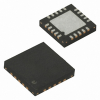
ATTINY43U-MU Atmel, ATTINY43U-MU Datasheet - Page 34

ATTINY43U-MU
Manufacturer Part Number
ATTINY43U-MU
Description
MCU AVR 4K FLASH 8MHZ 20-QFN
Manufacturer
Atmel
Series
AVR® ATtinyr
Specifications of ATTINY43U-MU
Core Processor
AVR
Core Size
8-Bit
Speed
8MHz
Connectivity
USI
Peripherals
Brown-out Detect/Reset, POR, PWM, Temp Sensor, WDT
Number Of I /o
16
Program Memory Size
4KB (2K x 16)
Program Memory Type
FLASH
Eeprom Size
64 x 8
Ram Size
256 x 8
Voltage - Supply (vcc/vdd)
1.8 V ~ 5.5 V
Data Converters
A/D 4x10b
Oscillator Type
Internal
Operating Temperature
-40°C ~ 85°C
Package / Case
20-MLF®, QFN
Processor Series
ATTINY4x
Core
AVR8
Data Bus Width
8 bit
Data Ram Size
256 B
Interface Type
SPI
Maximum Clock Frequency
8 MHz
Number Of Programmable I/os
16
Number Of Timers
2
Maximum Operating Temperature
+ 85 C
Mounting Style
SMD/SMT
3rd Party Development Tools
EWAVR, EWAVR-BL
Development Tools By Supplier
ATAVRDRAGON, ATSTK500, ATSTK600, ATAVRISP2, ATAVRONEKIT
Minimum Operating Temperature
- 40 C
On-chip Adc
10 bit, 4 Channel
For Use With
ATSTK600-TINYX3U - STK600 SOCKET/ADAPTER TINYX3U
Lead Free Status / RoHS Status
Lead free / RoHS Compliant
7.4.6
7.5
7.5.1
34
Register Description
ATtiny43U
Port Pins
MCUCR – MCU Control Register
When entering a sleep mode, all port pins should be configured to use minimum power. The
most important thing is then to ensure that no pins drive resistive loads. In sleep modes where
both the I/O clock (clk
will be disabled. This ensures that no power is consumed by the input logic when not needed. In
some cases, the input logic is needed for detecting wake-up conditions, and it will then be
enabled. See the section
which pins are enabled. If the input buffer is enabled and the input signal is left floating or has an
analog signal level close to V
For analog input pins, the digital input buffer should be disabled at all times. An analog signal
level close to V
input buffers can be disabled by writing to the Digital Input Disable Register (DIDR0). See
“DIDR0 – Digital Input Disable Register 0” on page 130
The MCU Control Register contains control bits for power management.
• Bit 7 – BODS: BOD Sleep
The BODS bit must be written to logic one in order to turn off BOD during sleep, see
on page
BODSE in MCUCR. To disable BOD in relevant sleep modes, both BODS and BODSE must first
be set to one. Then, to set the BODS bit, BODS must be set to one and BODSE must be set to
zero within four clock cycles.
The BODS bit is active three clock cycles after it is set. A sleep instruction must be executed
while BODS is active in order to turn off the BOD for the actual sleep mode. The BODS bit is
automatically cleared after three clock cycles.
• Bit 5 – SE: Sleep Enable
The SE bit must be written to logic one to make the MCU enter the sleep mode when the SLEEP
instruction is executed. To avoid the MCU entering the sleep mode unless it is the programmer’s
purpose, it is recommended to write the Sleep Enable (SE) bit to one just before the execution of
the SLEEP instruction and to clear it immediately after waking up.
• Bits 4, 3 – SM[1:0]: Sleep Mode Select Bits 2:0
These bits select between the three available sleep modes as shown in
Table 7-2.
Bit
0x35 (0x55)
Read/Write
Initial Value
SM1
0
31. Writing to the BODS bit is controlled by a timed sequence and an enable bit,
Sleep Mode Select
CC
BODS
R/W
7
0
/2 on an input pin can cause significant current even in active mode. Digital
I/O
) and the ADC clock (clk
PUD
R/W
SM0
6
0
“Digital Input Enable and Sleep Modes” on page 66
0
CC
/2, the input buffer will use excessive power.
R/W
SE
5
0
Sleep Mode
Idle
SM1
R/W
4
0
ADC
) are stopped, the input buffers of the device
SM0
R/W
3
0
for details.
BODSE
R/W
2
0
ISC01
R/W
1
0
Table 7-2
ISC00
R/W
0
0
for details on
8048B–AVR–03/09
below.
Table 7-1
MCUCR


