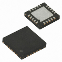
ATTINY43U-MU Atmel, ATTINY43U-MU Datasheet - Page 85

ATTINY43U-MU
Manufacturer Part Number
ATTINY43U-MU
Description
MCU AVR 4K FLASH 8MHZ 20-QFN
Manufacturer
Atmel
Series
AVR® ATtinyr
Specifications of ATTINY43U-MU
Core Processor
AVR
Core Size
8-Bit
Speed
8MHz
Connectivity
USI
Peripherals
Brown-out Detect/Reset, POR, PWM, Temp Sensor, WDT
Number Of I /o
16
Program Memory Size
4KB (2K x 16)
Program Memory Type
FLASH
Eeprom Size
64 x 8
Ram Size
256 x 8
Voltage - Supply (vcc/vdd)
1.8 V ~ 5.5 V
Data Converters
A/D 4x10b
Oscillator Type
Internal
Operating Temperature
-40°C ~ 85°C
Package / Case
20-MLF®, QFN
Processor Series
ATTINY4x
Core
AVR8
Data Bus Width
8 bit
Data Ram Size
256 B
Interface Type
SPI
Maximum Clock Frequency
8 MHz
Number Of Programmable I/os
16
Number Of Timers
2
Maximum Operating Temperature
+ 85 C
Mounting Style
SMD/SMT
3rd Party Development Tools
EWAVR, EWAVR-BL
Development Tools By Supplier
ATAVRDRAGON, ATSTK500, ATSTK600, ATAVRISP2, ATAVRONEKIT
Minimum Operating Temperature
- 40 C
On-chip Adc
10 bit, 4 Channel
For Use With
ATSTK600-TINYX3U - STK600 SOCKET/ADAPTER TINYX3U
Lead Free Status / RoHS Status
Lead free / RoHS Compliant
- Current page: 85 of 182
- Download datasheet (4Mb)
12.7.3
8048B–AVR–03/09
Fast PWM Mode
The timing diagram for the CTC mode is shown in
(TCNTn) increases until a Compare Match occurs between TCNTn and OCRnA, and then coun-
ter (TCNTn) is cleared.
Figure 12-5. CTC Mode, Timing Diagram
An interrupt can be generated each time the counter value reaches the TOP value by using the
OCFnA Flag. If the interrupt is enabled, the interrupt handler routine can be used for updating
the TOP value. However, changing TOP to a value close to BOTTOM when the counter is run-
ning with none or a low prescaler value must be done with care since the CTC mode does not
have the double buffering feature. If the new value written to OCRnA is lower than the current
value of TCNTn, the counter will miss the Compare Match. The counter will then have to count to
its maximum value (0xFF) and wrap around starting at 0x00 before the Compare Match can
occur.
For generating a waveform output in CTC mode, the OCnA output can be set to toggle its logical
level on each Compare Match by setting the Compare Output mode bits to toggle mode
(COMnA1:0 = 1). The OCnA value will not be visible on the port pin unless the data direction for
the pin is set to output. The waveform generated will have a maximum frequency of f
f
equation:
The N variable represents the prescale factor (1, 8, 64, 256, or 1024).
As for the Normal mode of operation, the TOVn Flag is set in the same timer clock cycle that the
counter counts from MAX to 0x00.
The fast Pulse Width Modulation or fast PWM mode (WGMn2:0 = 3 or 7) provides a high fre-
quency PWM waveform generation option. The fast PWM differs from the other PWM option by
its single-slope operation. The counter counts from BOTTOM to TOP then restarts from BOT-
TOM. TOP is defined as 0xFF when WGMn2:0 = 3, and OCRnA when WGMn2:0 = 7. In non-
inverting Compare Output mode, the Output Compare (OCnx) is cleared on the Compare Match
between TCNTn and OCRnx, and set at BOTTOM. In inverting Compare Output mode, the out-
put is set on Compare Match and cleared at BOTTOM. Due to the single-slope operation, the
operating frequency of the fast PWM mode can be twice as high as the phase correct PWM
mode that use dual-slope operation. This high frequency makes the fast PWM mode well suited
clk_I/O
TCNTn
OCn
(Toggle)
Period
/2 when OCRnA is set to zero (0x00). The waveform frequency is defined by the following
1
f
2
OCnx
=
------------------------------------------------- -
2 N
3
⋅
⋅
f
(
clk_I/O
1
+
Figure 12-5 on page
4
OCRnx
)
85. The counter value
OCnx Interrupt Flag Set
(COMnx1:0 = 1)
OCnx
85
=
Related parts for ATTINY43U-MU
Image
Part Number
Description
Manufacturer
Datasheet
Request
R

Part Number:
Description:
Manufacturer:
Atmel Corporation
Datasheet:

Part Number:
Description:
Microcontrollers (MCU) 512B FL 32B SRAM TIMER ATTINY4 12MHz
Manufacturer:
Atmel

Part Number:
Description:
IC MCU AVR 512B FLASH SOT-23-6
Manufacturer:
Atmel
Datasheet:

Part Number:
Description:
IC MCU AVR 512B FLASH SOT-23-6
Manufacturer:
Atmel
Datasheet:

Part Number:
Description:
DEV KIT FOR AVR/AVR32
Manufacturer:
Atmel
Datasheet:

Part Number:
Description:
INTERVAL AND WIPE/WASH WIPER CONTROL IC WITH DELAY
Manufacturer:
ATMEL Corporation
Datasheet:

Part Number:
Description:
Low-Voltage Voice-Switched IC for Hands-Free Operation
Manufacturer:
ATMEL Corporation
Datasheet:

Part Number:
Description:
MONOLITHIC INTEGRATED FEATUREPHONE CIRCUIT
Manufacturer:
ATMEL Corporation
Datasheet:

Part Number:
Description:
AM-FM Receiver IC U4255BM-M
Manufacturer:
ATMEL Corporation
Datasheet:

Part Number:
Description:
Monolithic Integrated Feature Phone Circuit
Manufacturer:
ATMEL Corporation
Datasheet:

Part Number:
Description:
Multistandard Video-IF and Quasi Parallel Sound Processing
Manufacturer:
ATMEL Corporation
Datasheet:


