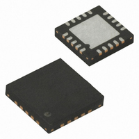
ATTINY43U-MU Atmel, ATTINY43U-MU Datasheet - Page 155

ATTINY43U-MU
Manufacturer Part Number
ATTINY43U-MU
Description
MCU AVR 4K FLASH 8MHZ 20-QFN
Manufacturer
Atmel
Series
AVR® ATtinyr
Specifications of ATTINY43U-MU
Core Processor
AVR
Core Size
8-Bit
Speed
8MHz
Connectivity
USI
Peripherals
Brown-out Detect/Reset, POR, PWM, Temp Sensor, WDT
Number Of I /o
16
Program Memory Size
4KB (2K x 16)
Program Memory Type
FLASH
Eeprom Size
64 x 8
Ram Size
256 x 8
Voltage - Supply (vcc/vdd)
1.8 V ~ 5.5 V
Data Converters
A/D 4x10b
Oscillator Type
Internal
Operating Temperature
-40°C ~ 85°C
Package / Case
20-MLF®, QFN
Processor Series
ATTINY4x
Core
AVR8
Data Bus Width
8 bit
Data Ram Size
256 B
Interface Type
SPI
Maximum Clock Frequency
8 MHz
Number Of Programmable I/os
16
Number Of Timers
2
Maximum Operating Temperature
+ 85 C
Mounting Style
SMD/SMT
3rd Party Development Tools
EWAVR, EWAVR-BL
Development Tools By Supplier
ATAVRDRAGON, ATSTK500, ATSTK600, ATAVRISP2, ATAVRONEKIT
Minimum Operating Temperature
- 40 C
On-chip Adc
10 bit, 4 Channel
For Use With
ATSTK600-TINYX3U - STK600 SOCKET/ADAPTER TINYX3U
Lead Free Status / RoHS Status
Lead free / RoHS Compliant
- Current page: 155 of 182
- Download datasheet (4Mb)
20. Electrical Characteristics
20.1
20.2
Note:
Table 20-1.
8048B–AVR–03/09
Operating Temperature.................................. -55°C to +125°C
Storage Temperature ..................................... -65°C to +150°C
Voltage on any Pin except RESET
with respect to Ground ................................-0.5V to V
Voltage on RESET with respect to Ground......-0.5V to +13.0V
Maximum Operating Voltage ............................................ 6.0V
DC Current per I/O Pin ............................................... 40.0 mA
DC Current
Symbol
V
V
V
I
V
I
LIH
LIL
OH
OL
IH
IL
Absolute Maximum Ratings*
DC Characteristics
All DC Characteristics contained in this data sheet are based on simulation and characterization of other AVR microcontrollers
manufactured in the same process technology. These values are preliminary values representing design targets, and will be
updated after characterization of actual silicon.
Parameter
Input Low Voltage,
Any Pin as I/O
Input Low Voltage,
RESET Pin as Reset
Input High-voltage,
Any Pin as I/O
Input High-voltage,
RESET Pin as Reset
Output Low Voltage
Pins PB1, PB2, PB4 and PB5
Output Low Voltage
All Other I/O Pins, except RESET
pin
Output High-voltage
All I/O Pins, except RESET pin
Input Leakage Current, I/O Pin
Input Leakage Current, I/O Pin
V
CC
DC Characteristics. T
and GND Pins................................ 200.0 mA
(4)
(4)
(6)
(2)
(2)
,
,
A
= -40°C to 85°C
(5)
V
V
V
V
V
V
I
I
I
I
I
I
I
I
I
V
V
Condition
OL
OL
OL
OL
OL
OL
OH
OH
OH
CC
CC
CC
CC
CC
CC
CC
CC
= 20 mA, V
= 10 mA, V
= 4 mA, V
= 10 mA, V
= 5 mA, V
= 2 mA, V
= 10 mA, V
= 5 mA, V
= 2 mA, V
= 1.8V - 2.4V
= 2.4V - 5.5V
= 1.8V - 5.5V
= 1.8V - 2.4V
= 2.4V - 5.5V
=
=
CC
= 1.8V to 5.5V
5.5
5.5
+0.5V
V, pin low
V, pin high
CC
CC
CC
CC
CC
CC
CC
CC
CC
= 1.8V
= 3V
= 1.8V
= 3V
= 1.8V
= 5V
= 3V
= 5V
= 5V
*NOTICE:
0.9 V
0.7V
0.6V
Stresses beyond those listed under “Absolute
Maximum Ratings” may cause permanent dam-
age to the device. This is a stress rating only and
functional operation of the device at these or
other conditions beyond those indicated in the
operational sections of this specification is not
implied. Exposure to absolute maximum rating
conditions for extended periods may affect
device reliability.
Min.
-0.5
-0.5
-0.5
4.0
2.3
1.4
-1
-1
CC
CC
CC
(3)
(3)
(3)
Typ.
0.2V
0.3V
0.2V
V
V
V
CC
CC
CC
Max.
0.8
0.8
0.8
0.8
0.8
0.8
1
1
CC
CC
CC
+0.5
+0.5
+0.5
(1)
(1)
(1)
Units
µA
µA
V
V
V
V
V
V
V
V
V
V
V
V
V
V
V
155
Related parts for ATTINY43U-MU
Image
Part Number
Description
Manufacturer
Datasheet
Request
R

Part Number:
Description:
Manufacturer:
Atmel Corporation
Datasheet:

Part Number:
Description:
Microcontrollers (MCU) 512B FL 32B SRAM TIMER ATTINY4 12MHz
Manufacturer:
Atmel

Part Number:
Description:
IC MCU AVR 512B FLASH SOT-23-6
Manufacturer:
Atmel
Datasheet:

Part Number:
Description:
IC MCU AVR 512B FLASH SOT-23-6
Manufacturer:
Atmel
Datasheet:

Part Number:
Description:
DEV KIT FOR AVR/AVR32
Manufacturer:
Atmel
Datasheet:

Part Number:
Description:
INTERVAL AND WIPE/WASH WIPER CONTROL IC WITH DELAY
Manufacturer:
ATMEL Corporation
Datasheet:

Part Number:
Description:
Low-Voltage Voice-Switched IC for Hands-Free Operation
Manufacturer:
ATMEL Corporation
Datasheet:

Part Number:
Description:
MONOLITHIC INTEGRATED FEATUREPHONE CIRCUIT
Manufacturer:
ATMEL Corporation
Datasheet:

Part Number:
Description:
AM-FM Receiver IC U4255BM-M
Manufacturer:
ATMEL Corporation
Datasheet:

Part Number:
Description:
Monolithic Integrated Feature Phone Circuit
Manufacturer:
ATMEL Corporation
Datasheet:

Part Number:
Description:
Multistandard Video-IF and Quasi Parallel Sound Processing
Manufacturer:
ATMEL Corporation
Datasheet:


