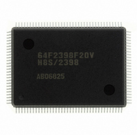
DF2398F20V Renesas Electronics America, DF2398F20V Datasheet - Page 143

DF2398F20V
Manufacturer Part Number
DF2398F20V
Description
IC H8S/2300 MCU FLASH 128QFP
Manufacturer
Renesas Electronics America
Series
H8® H8S/2300r
Specifications of DF2398F20V
Core Processor
H8S/2000
Core Size
16-Bit
Speed
20MHz
Connectivity
SCI, SmartCard
Peripherals
DMA, POR, PWM, WDT
Number Of I /o
87
Program Memory Size
256KB (256K x 8)
Program Memory Type
FLASH
Ram Size
8K x 8
Voltage - Supply (vcc/vdd)
4.5 V ~ 5.5 V
Data Converters
A/D 8x10b; D/A 2x8b
Oscillator Type
Internal
Operating Temperature
-20°C ~ 75°C
Package / Case
128-QFP
For Use With
YR0K42378FC000BA - KIT EVAL FOR H8S/2378
Lead Free Status / RoHS Status
Lead free / RoHS Compliant
Eeprom Size
-
Available stocks
Company
Part Number
Manufacturer
Quantity
Price
Company:
Part Number:
DF2398F20V
Manufacturer:
Renesas Electronics America
Quantity:
135
Company:
Part Number:
DF2398F20V
Manufacturer:
Renesas Electronics America
Quantity:
10 000
- Current page: 143 of 1049
- Download datasheet (5Mb)
6.2.4
BCRH is an 8-bit readable/writable register that selects enabling or disabling of idle cycle insertion, and the memory
interface for areas 2 to 5 and area 0.
BCRH is initialized to H'D0 by a power-on reset and in hardware standby mode. It is not initialized by a manual reset* or
in software standby mode.
Note: * Manual reset is only supported in the H8S/2357 ZTAT.
Bit 7—Idle Cycle Insert 1 (ICIS1): Selects whether or not one idle cycle state is to be inserted between bus cycles when
successive external read cycles are performed in different areas.
Bit 6—Idle Cycle Insert 0 (ICIS0): Selects whether or not one idle cycle state is to be inserted between bus cycles when
successive external read and external write cycles are performed .
Bit 5—Burst ROM Enable (BRSTRM): Selects whether area 0 is used as a burst ROM interface.
Bit 4—Burst Cycle Select 1 (BRSTS1): Selects the number of burst cycles for the burst ROM interface.
Bit
Initial value :
R/W
Bus Control Register H (BCRH)
Bit 7
ICIS1
0
1
Bit 6
ICIS0
0
1
Bit 5
BRSTRM
0
1
Bit 4
BRSTS1
0
1
:
:
ICIS1
R/W
7
1
Description
Idle cycle not inserted in case of successive external read cycles in different areas
Idle cycle inserted in case of successive external read cycles in different areas
Description
Idle cycle not inserted in case of successive external read and external write cycles
Idle cycle inserted in case of successive external read and external write cycles
Description
Area 0 is basic bus interface
Area 0 is burst ROM interface
Description
Burst cycle comprises 1 state
Burst cycle comprises 2 states
ICIS0
R/W
6
1
BRSTRM BRSTS1 BRSTS0
R/W
5
0
R/W
4
1
R/W
3
0
RMTS2
R/W
2
0
RMTS1
R/W
Rev.6.00 Oct.28.2004 page 113 of 1016
1
0
RMTS0
R/W
0
0
(Initial value)
(Initial value)
(Initial value)
(Initial value)
REJ09B0138-0600H
Related parts for DF2398F20V
Image
Part Number
Description
Manufacturer
Datasheet
Request
R

Part Number:
Description:
CONN PLUG 12POS DUAL 0.5MM SMD
Manufacturer:
Hirose Electric Co Ltd
Datasheet:

Part Number:
Description:
CONN PLUG 18POS DUAL 0.5MM SMD
Manufacturer:
Hirose Electric Co Ltd
Datasheet:

Part Number:
Description:
CONN PLUG 14POS DUAL 0.5MM SMD
Manufacturer:
Hirose Electric Co Ltd
Datasheet:

Part Number:
Description:
CONN RECEPT 20POS DUAL 0.5MM SMD
Manufacturer:
Hirose Electric Co Ltd
Datasheet:

Part Number:
Description:
CONN PLUG 16POS DUAL 0.5MM SMD
Manufacturer:
Hirose Electric Co Ltd
Datasheet:

Part Number:
Description:
CONN RECEPT 16POS DUAL 0.5MM SMD
Manufacturer:
Hirose Electric Co Ltd
Datasheet:

Part Number:
Description:
CONN PLUG 20POS DUAL 0.5MM SMD
Manufacturer:
Hirose Electric Co Ltd
Datasheet:

Part Number:
Description:
CONN PLUG 30POS DUAL 0.5MM SMD
Manufacturer:
Hirose Electric Co Ltd
Datasheet:

Part Number:
Description:
CONN RECEPT 30POS DUAL 0.5MM SMD
Manufacturer:
Hirose Electric Co Ltd
Datasheet:

Part Number:
Description:
CONN PLUG 40POS DUAL 0.5MM SMD
Manufacturer:
Hirose Electric Co Ltd
Datasheet:

Part Number:
Description:
KIT STARTER FOR M16C/29
Manufacturer:
Renesas Electronics America
Datasheet:

Part Number:
Description:
KIT STARTER FOR R8C/2D
Manufacturer:
Renesas Electronics America
Datasheet:

Part Number:
Description:
R0K33062P STARTER KIT
Manufacturer:
Renesas Electronics America
Datasheet:

Part Number:
Description:
KIT STARTER FOR R8C/23 E8A
Manufacturer:
Renesas Electronics America
Datasheet:

Part Number:
Description:
KIT STARTER FOR R8C/25
Manufacturer:
Renesas Electronics America
Datasheet:


