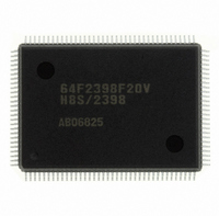
DF2398F20V Renesas Electronics America, DF2398F20V Datasheet - Page 614

DF2398F20V
Manufacturer Part Number
DF2398F20V
Description
IC H8S/2300 MCU FLASH 128QFP
Manufacturer
Renesas Electronics America
Series
H8® H8S/2300r
Specifications of DF2398F20V
Core Processor
H8S/2000
Core Size
16-Bit
Speed
20MHz
Connectivity
SCI, SmartCard
Peripherals
DMA, POR, PWM, WDT
Number Of I /o
87
Program Memory Size
256KB (256K x 8)
Program Memory Type
FLASH
Ram Size
8K x 8
Voltage - Supply (vcc/vdd)
4.5 V ~ 5.5 V
Data Converters
A/D 8x10b; D/A 2x8b
Oscillator Type
Internal
Operating Temperature
-20°C ~ 75°C
Package / Case
128-QFP
For Use With
YR0K42378FC000BA - KIT EVAL FOR H8S/2378
Lead Free Status / RoHS Status
Lead free / RoHS Compliant
Eeprom Size
-
Available stocks
Company
Part Number
Manufacturer
Quantity
Price
Company:
Part Number:
DF2398F20V
Manufacturer:
Renesas Electronics America
Quantity:
135
Company:
Part Number:
DF2398F20V
Manufacturer:
Renesas Electronics America
Quantity:
10 000
- Current page: 614 of 1049
- Download datasheet (5Mb)
19.7.2
FLMCR2 is an 8-bit register that monitors the presence or absence of flash memory program/erase protection (error
protection) and performs setup for flash memory program/erase mode. FLMCR2 is initialized to H'00 by a reset, and in
hardware standby mode. The ESU and PSU bits are cleared to 0 in software standby mode, hardware protect mode, and
software protect mode.
When on-chip flash memory is disabled, a read will return H'00.
Bit 7—Flash Memory Error (FLER): Indicates that an error has occurred during an operation on flash memory
(programming or erasing). When FLER is set to 1, flash memory goes to the error-protection state.
Bits 6 to 2—Reserved: These bits cannot be modified and are always read as 0.
Bit 1—Erase Setup (ESU): Prepares for a transition to erase mode. Set this bit to 1 before setting the E bit to 1 in
FLMCR1. Do not set the SWE, PSU, EV, PV, E, or P bit at the same time.
Bit 0—Program Setup (PSU): Prepares for a transition to program mode. Set this bit to 1 before setting the P bit to 1 in
FLMCR1. Do not set the SWE, ESU, EV, PV, E, or P bit at the same time.
Rev.6.00 Oct.28.2004 page 584 of 1016
REJ09B0138-0600H
Bit
Initial value
Read/Write
Flash Memory Control Register 2 (FLMCR2)
Bit 7
FLER
0
1
Bit 1
ESU
0
1
FLER
7
0
R
Description
Flash memory is operating normally
Flash memory program/erase protection (error protection) is disabled
[Clearing condition]
Reset or hardware standby mode
An error has occurred during flash memory programming/erasing
Flash memory program/erase protection (error protection) is enabled
[Setting condition]
See section 19.10.3, Error Protection
Description
Erase setup cleared
Erase setup
[Setting condition]
When FWE = 1, and SWE = 1
—
—
6
0
—
—
5
0
—
—
4
0
—
—
3
0
—
—
2
0
ESU
R/W
1
0
PSU
R/W
0
0
(Initial value)
(Initial value)
Related parts for DF2398F20V
Image
Part Number
Description
Manufacturer
Datasheet
Request
R

Part Number:
Description:
CONN PLUG 12POS DUAL 0.5MM SMD
Manufacturer:
Hirose Electric Co Ltd
Datasheet:

Part Number:
Description:
CONN PLUG 18POS DUAL 0.5MM SMD
Manufacturer:
Hirose Electric Co Ltd
Datasheet:

Part Number:
Description:
CONN PLUG 14POS DUAL 0.5MM SMD
Manufacturer:
Hirose Electric Co Ltd
Datasheet:

Part Number:
Description:
CONN RECEPT 20POS DUAL 0.5MM SMD
Manufacturer:
Hirose Electric Co Ltd
Datasheet:

Part Number:
Description:
CONN PLUG 16POS DUAL 0.5MM SMD
Manufacturer:
Hirose Electric Co Ltd
Datasheet:

Part Number:
Description:
CONN RECEPT 16POS DUAL 0.5MM SMD
Manufacturer:
Hirose Electric Co Ltd
Datasheet:

Part Number:
Description:
CONN PLUG 20POS DUAL 0.5MM SMD
Manufacturer:
Hirose Electric Co Ltd
Datasheet:

Part Number:
Description:
CONN PLUG 30POS DUAL 0.5MM SMD
Manufacturer:
Hirose Electric Co Ltd
Datasheet:

Part Number:
Description:
CONN RECEPT 30POS DUAL 0.5MM SMD
Manufacturer:
Hirose Electric Co Ltd
Datasheet:

Part Number:
Description:
CONN PLUG 40POS DUAL 0.5MM SMD
Manufacturer:
Hirose Electric Co Ltd
Datasheet:

Part Number:
Description:
KIT STARTER FOR M16C/29
Manufacturer:
Renesas Electronics America
Datasheet:

Part Number:
Description:
KIT STARTER FOR R8C/2D
Manufacturer:
Renesas Electronics America
Datasheet:

Part Number:
Description:
R0K33062P STARTER KIT
Manufacturer:
Renesas Electronics America
Datasheet:

Part Number:
Description:
KIT STARTER FOR R8C/23 E8A
Manufacturer:
Renesas Electronics America
Datasheet:

Part Number:
Description:
KIT STARTER FOR R8C/25
Manufacturer:
Renesas Electronics America
Datasheet:


