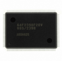
DF2398F20V Renesas Electronics America, DF2398F20V Datasheet - Page 565

DF2398F20V
Manufacturer Part Number
DF2398F20V
Description
IC H8S/2300 MCU FLASH 128QFP
Manufacturer
Renesas Electronics America
Series
H8® H8S/2300r
Specifications of DF2398F20V
Core Processor
H8S/2000
Core Size
16-Bit
Speed
20MHz
Connectivity
SCI, SmartCard
Peripherals
DMA, POR, PWM, WDT
Number Of I /o
87
Program Memory Size
256KB (256K x 8)
Program Memory Type
FLASH
Ram Size
8K x 8
Voltage - Supply (vcc/vdd)
4.5 V ~ 5.5 V
Data Converters
A/D 8x10b; D/A 2x8b
Oscillator Type
Internal
Operating Temperature
-20°C ~ 75°C
Package / Case
128-QFP
For Use With
YR0K42378FC000BA - KIT EVAL FOR H8S/2378
Lead Free Status / RoHS Status
Lead free / RoHS Compliant
Eeprom Size
-
Available stocks
Company
Part Number
Manufacturer
Quantity
Price
Company:
Part Number:
DF2398F20V
Manufacturer:
Renesas Electronics America
Quantity:
135
Company:
Part Number:
DF2398F20V
Manufacturer:
Renesas Electronics America
Quantity:
10 000
- Current page: 565 of 1049
- Download datasheet (5Mb)
Powering On: To secure the clock duty from power-on, the following switching procedure should be followed.
[1] The initial state is port input and high impedance. Use a pull-up resistor or pull-down resistor to fix the potential.
[2] Fix the SCK pin to the specified output level with the CKE1 bit in SCR.
[3] Set SMR and SCMR, and switch to Smart Card mode operation.
[4] Set the CKE0 bit in SCR to 1 to start clock output.
15.4
The following points should be noted when using the SCI as a Smart Card interface.
Receive Data Sampling Timing and Reception Margin in Smart Card Interface Mode: In Smart Card Interface mode,
the SCI operates on a basic clock with a frequency of 372 times the transfer rate.
In reception, the SCI samples the falling edge of the start bit using the basic clock, and performs internal synchronization.
Receive data is latched internally at the rising edge of the 186th pulse of the basic clock. This is illustrated in figure 15-10.
Thus the reception margin in asynchronous mode is given by the following formula.
Usage Notes
Internal
basic
clock
Receive
data (RxD)
Synchro-
nization
sampling
timing
Data
sampling
timing
Figure 15-10 Receive Data Sampling Timing in Smart Card Mode
[1] [2] [3]
0
186 clocks
Normal operation
Figure 15-9 Clock Halt and Restart Procedure
185
372 clocks
Start bit
371
[4] [5] [6]
0
Software
standby
D0
[7] [8] [9]
Normal operation
185
Rev.6.00 Oct.28.2004 page 535 of 1016
371 0
D1
REJ09B0138-0600H
Related parts for DF2398F20V
Image
Part Number
Description
Manufacturer
Datasheet
Request
R

Part Number:
Description:
CONN PLUG 12POS DUAL 0.5MM SMD
Manufacturer:
Hirose Electric Co Ltd
Datasheet:

Part Number:
Description:
CONN PLUG 18POS DUAL 0.5MM SMD
Manufacturer:
Hirose Electric Co Ltd
Datasheet:

Part Number:
Description:
CONN PLUG 14POS DUAL 0.5MM SMD
Manufacturer:
Hirose Electric Co Ltd
Datasheet:

Part Number:
Description:
CONN RECEPT 20POS DUAL 0.5MM SMD
Manufacturer:
Hirose Electric Co Ltd
Datasheet:

Part Number:
Description:
CONN PLUG 16POS DUAL 0.5MM SMD
Manufacturer:
Hirose Electric Co Ltd
Datasheet:

Part Number:
Description:
CONN RECEPT 16POS DUAL 0.5MM SMD
Manufacturer:
Hirose Electric Co Ltd
Datasheet:

Part Number:
Description:
CONN PLUG 20POS DUAL 0.5MM SMD
Manufacturer:
Hirose Electric Co Ltd
Datasheet:

Part Number:
Description:
CONN PLUG 30POS DUAL 0.5MM SMD
Manufacturer:
Hirose Electric Co Ltd
Datasheet:

Part Number:
Description:
CONN RECEPT 30POS DUAL 0.5MM SMD
Manufacturer:
Hirose Electric Co Ltd
Datasheet:

Part Number:
Description:
CONN PLUG 40POS DUAL 0.5MM SMD
Manufacturer:
Hirose Electric Co Ltd
Datasheet:

Part Number:
Description:
KIT STARTER FOR M16C/29
Manufacturer:
Renesas Electronics America
Datasheet:

Part Number:
Description:
KIT STARTER FOR R8C/2D
Manufacturer:
Renesas Electronics America
Datasheet:

Part Number:
Description:
R0K33062P STARTER KIT
Manufacturer:
Renesas Electronics America
Datasheet:

Part Number:
Description:
KIT STARTER FOR R8C/23 E8A
Manufacturer:
Renesas Electronics America
Datasheet:

Part Number:
Description:
KIT STARTER FOR R8C/25
Manufacturer:
Renesas Electronics America
Datasheet:


