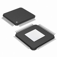
PIC24FJ256DA206-I/MR Microchip Technology, PIC24FJ256DA206-I/MR Datasheet - Page 143

PIC24FJ256DA206-I/MR
Manufacturer Part Number
PIC24FJ256DA206-I/MR
Description
MCU PIC 16BIT FLASH 256K 64VQFN
Manufacturer
Microchip Technology
Series
PIC® 24Fr
Specifications of PIC24FJ256DA206-I/MR
Program Memory Type
FLASH
Program Memory Size
256KB (85.5K x 24)
Package / Case
64-VFQFN, Exposed Pad
Core Processor
PIC
Core Size
16-Bit
Speed
32MHz
Connectivity
I²C, IrDA, SPI, UART/USART, USB OTG
Peripherals
Brown-out Detect/Reset, GFX, LVD, POR, PWM, WDT
Number Of I /o
52
Ram Size
96K x 8
Voltage - Supply (vcc/vdd)
2.2 V ~ 3.6 V
Data Converters
A/D 16x10b
Oscillator Type
Internal
Operating Temperature
-40°C ~ 85°C
Processor Series
PIC24FJ
Core
PIC
Data Bus Width
16 bit
Data Ram Size
96 KB
Interface Type
UART, SPI, USB, I2C, RS-485, RS-232
Maximum Clock Frequency
32 MHz
Number Of Programmable I/os
23
Number Of Timers
5
Operating Supply Voltage
3.6 V
Maximum Operating Temperature
+ 85 C
Mounting Style
SMD/SMT
3rd Party Development Tools
52713-733, 52714-737, 53276-922, EWDSPIC
Development Tools By Supplier
PG164130, DV164035, DV244005, DV164005, AC164127-4, AC164127-6, AC164139, DM240001, DM240312, DV164039
Minimum Operating Temperature
- 40 C
Lead Free Status / RoHS Status
Lead free / RoHS Compliant
Eeprom Size
-
Lead Free Status / Rohs Status
Lead free / RoHS Compliant
- Current page: 143 of 408
- Download datasheet (4Mb)
8.3
The following five Special Function Registers control
the operation of the oscillator:
• OSCCON
• CLKDIV
• OSCTUN
• CLKDIV2
• REFOCON
REGISTER 8-1:
2010 Microchip Technology Inc.
bit 15
bit 7
Legend:
R = Readable bit
-n = Value at POR
HS = Hardware Settable bit
bit 15
bit 14-12
bit 11
Note 1:
CLKLOCK
R/S-0
U-0
—
2:
3:
Control Registers
Reset values for these bits are determined by the FNOSC Configuration bits.
The state of the IOLOCK bit can only be changed once an unlocking sequence has been executed. In
addition, if the IOL1WAY Configuration bit is ‘1’, once the IOLOCK bit is set, it cannot be cleared.
Also resets to ‘0’ during any valid clock switch or whenever a non PLL Clock mode is selected.
R-x, HSC
Unimplemented: Read as ‘0’
COSC<2:0>: Current Oscillator Selection bits
111 = Fast RC Oscillator with Postscaler (FRCDIV)
110 = Fast RC/16 Oscillator
101 = Low-Power RC Oscillator (LPRC)
100 = Secondary Oscillator (SOSC)
011 = Primary Oscillator with PLL module (XTPLL, HSPLL, ECPLL)
010 = Primary Oscillator (XT, HS, EC)
001 = Fast RC Oscillator with Postscaler and PLL module (FRCPLL)
000 = Fast RC Oscillator (FRC)
Unimplemented: Read as ‘0’
IOLOCK
COSC2
R/W-0
OSCCON: OSCILLATOR CONTROL REGISTER
(2)
(1)
C = Clearable bit
W = Writable bit
‘1’ = Bit is set
R-x, HSC
R-0, HSC
COSC1
LOCK
(1)
(3)
R-x, HSC
COSC0
U-0
—
PIC24FJ256DA210 FAMILY
(1)
S = Settable bit
U = Unimplemented bit, read as ‘0’
‘0’ = Bit is cleared
R/C-0, HS
U-0
CF
—
(1)
The OSCCON register (Register 8-1) is the main con-
trol register for the oscillator. It controls clock source
switching and allows the monitoring of clock sources.
The CLKDIV register (Register 8-2) controls the
features associated with Doze mode, as well as the
postscaler for the FRC oscillator.
The OSCTUN register (Register 8-3) allows the user to
fine tune the FRC oscillator over a range of
approximately ±1.5%.
The CLKDIV2 register (Register 8-4) controls the clock
to the display glass, with the frequency ranging from
750 kHz to 96 MHz.
The REFOCON register (Register 8-5) controls the
frequency of the reference clock out.
POSCEN
R/W-x
NOSC2
R/W-0
(1)
x = Bit is unknown
HSC = Hardware Settable/Clearable bit
SOSCEN
R/W-x
NOSC1
R/W-0
(1)
DS39969B-page 143
R/W-x
OSWEN
NOSC0
R/W-0
(1)
bit 8
bit 0
Related parts for PIC24FJ256DA206-I/MR
Image
Part Number
Description
Manufacturer
Datasheet
Request
R

Part Number:
Description:
Manufacturer:
Microchip Technology Inc.
Datasheet:

Part Number:
Description:
Manufacturer:
Microchip Technology Inc.
Datasheet:

Part Number:
Description:
Manufacturer:
Microchip Technology Inc.
Datasheet:

Part Number:
Description:
Manufacturer:
Microchip Technology Inc.
Datasheet:

Part Number:
Description:
Manufacturer:
Microchip Technology Inc.
Datasheet:

Part Number:
Description:
Manufacturer:
Microchip Technology Inc.
Datasheet:

Part Number:
Description:
Manufacturer:
Microchip Technology Inc.
Datasheet:

Part Number:
Description:
Manufacturer:
Microchip Technology Inc.
Datasheet:


