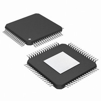
PIC24FJ256DA206-I/MR Microchip Technology, PIC24FJ256DA206-I/MR Datasheet - Page 371

PIC24FJ256DA206-I/MR
Manufacturer Part Number
PIC24FJ256DA206-I/MR
Description
MCU PIC 16BIT FLASH 256K 64VQFN
Manufacturer
Microchip Technology
Series
PIC® 24Fr
Specifications of PIC24FJ256DA206-I/MR
Program Memory Type
FLASH
Program Memory Size
256KB (85.5K x 24)
Package / Case
64-VFQFN, Exposed Pad
Core Processor
PIC
Core Size
16-Bit
Speed
32MHz
Connectivity
I²C, IrDA, SPI, UART/USART, USB OTG
Peripherals
Brown-out Detect/Reset, GFX, LVD, POR, PWM, WDT
Number Of I /o
52
Ram Size
96K x 8
Voltage - Supply (vcc/vdd)
2.2 V ~ 3.6 V
Data Converters
A/D 16x10b
Oscillator Type
Internal
Operating Temperature
-40°C ~ 85°C
Processor Series
PIC24FJ
Core
PIC
Data Bus Width
16 bit
Data Ram Size
96 KB
Interface Type
UART, SPI, USB, I2C, RS-485, RS-232
Maximum Clock Frequency
32 MHz
Number Of Programmable I/os
23
Number Of Timers
5
Operating Supply Voltage
3.6 V
Maximum Operating Temperature
+ 85 C
Mounting Style
SMD/SMT
3rd Party Development Tools
52713-733, 52714-737, 53276-922, EWDSPIC
Development Tools By Supplier
PG164130, DV164035, DV244005, DV164005, AC164127-4, AC164127-6, AC164139, DM240001, DM240312, DV164039
Minimum Operating Temperature
- 40 C
Lead Free Status / RoHS Status
Lead free / RoHS Compliant
Eeprom Size
-
Lead Free Status / Rohs Status
Lead free / RoHS Compliant
- Current page: 371 of 408
- Download datasheet (4Mb)
30.0
This section provides an overview of the PIC24FJ256DA210 family electrical characteristics. Additional information will
be provided in future revisions of this document as it becomes available.
Absolute maximum ratings for the PIC24FJ256DA210 family are listed below. Exposure to these maximum rating
conditions for extended periods may affect device reliability. Functional operation of the device at these, or any other
conditions above the parameters indicated in the operation listings of this specification, is not implied.
Absolute Maximum Ratings
Ambient temperature under bias.............................................................................................................-40°C to +100°C
Storage temperature .............................................................................................................................. -65°C to +150°C
Voltage on V
Voltage on any combined analog and digital pin and MCLR, with respect to V
Voltage on any digital only pin with respect to V
Voltage on any digital only pin with respect to V
Voltage on V
Maximum current out of V
Maximum current into V
Maximum output current sunk by any I/O pin..........................................................................................................25 mA
Maximum output current sourced by any I/O pin ....................................................................................................25 mA
Maximum current sunk by all ports .......................................................................................................................200 mA
Maximum current sourced by all ports (Note 1)....................................................................................................200 mA
2010 Microchip Technology Inc.
†NOTICE: Stresses above those listed under “Absolute Maximum Ratings” may cause permanent damage to the
device. This is a stress rating only and functional operation of the device at those or any other conditions above those
indicated in the operation listings of this specification is not implied. Exposure to maximum rating conditions for
extended periods may affect device reliability.
Note 1: Maximum allowable current is a function of device maximum power dissipation (see Table 30-1).
ELECTRICAL CHARACTERISTICS
DD
BUS
with respect to V
pin with respect to V
DD
SS
pin (Note 1)................................................................................................................250 mA
pin ...........................................................................................................................300 mA
SS
(†)
......................................................................................................... -0.3V to +4.0V
SS
, independent of V
SS
SS
PIC24FJ256DA210 FAMILY
when V
when V
DD
DD
DD
< 3.0V............................................ -0.3V to (V
> 3.0V..................................................... -0.3V to (+5.5V)
or V
USB
................................................. -0.3V to (+5.5V)
SS
......................... -0.3V to (V
DS39969B-page 371
DD
DD
+ 0.3V)
+ 0.3V)
Related parts for PIC24FJ256DA206-I/MR
Image
Part Number
Description
Manufacturer
Datasheet
Request
R

Part Number:
Description:
Manufacturer:
Microchip Technology Inc.
Datasheet:

Part Number:
Description:
Manufacturer:
Microchip Technology Inc.
Datasheet:

Part Number:
Description:
Manufacturer:
Microchip Technology Inc.
Datasheet:

Part Number:
Description:
Manufacturer:
Microchip Technology Inc.
Datasheet:

Part Number:
Description:
Manufacturer:
Microchip Technology Inc.
Datasheet:

Part Number:
Description:
Manufacturer:
Microchip Technology Inc.
Datasheet:

Part Number:
Description:
Manufacturer:
Microchip Technology Inc.
Datasheet:

Part Number:
Description:
Manufacturer:
Microchip Technology Inc.
Datasheet:


