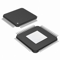
PIC24FJ256DA206-I/MR Microchip Technology, PIC24FJ256DA206-I/MR Datasheet - Page 152

PIC24FJ256DA206-I/MR
Manufacturer Part Number
PIC24FJ256DA206-I/MR
Description
MCU PIC 16BIT FLASH 256K 64VQFN
Manufacturer
Microchip Technology
Series
PIC® 24Fr
Specifications of PIC24FJ256DA206-I/MR
Program Memory Type
FLASH
Program Memory Size
256KB (85.5K x 24)
Package / Case
64-VFQFN, Exposed Pad
Core Processor
PIC
Core Size
16-Bit
Speed
32MHz
Connectivity
I²C, IrDA, SPI, UART/USART, USB OTG
Peripherals
Brown-out Detect/Reset, GFX, LVD, POR, PWM, WDT
Number Of I /o
52
Ram Size
96K x 8
Voltage - Supply (vcc/vdd)
2.2 V ~ 3.6 V
Data Converters
A/D 16x10b
Oscillator Type
Internal
Operating Temperature
-40°C ~ 85°C
Processor Series
PIC24FJ
Core
PIC
Data Bus Width
16 bit
Data Ram Size
96 KB
Interface Type
UART, SPI, USB, I2C, RS-485, RS-232
Maximum Clock Frequency
32 MHz
Number Of Programmable I/os
23
Number Of Timers
5
Operating Supply Voltage
3.6 V
Maximum Operating Temperature
+ 85 C
Mounting Style
SMD/SMT
3rd Party Development Tools
52713-733, 52714-737, 53276-922, EWDSPIC
Development Tools By Supplier
PG164130, DV164035, DV244005, DV164005, AC164127-4, AC164127-6, AC164139, DM240001, DM240312, DV164039
Minimum Operating Temperature
- 40 C
Lead Free Status / RoHS Status
Lead free / RoHS Compliant
Eeprom Size
-
Lead Free Status / Rohs Status
Lead free / RoHS Compliant
- Current page: 152 of 408
- Download datasheet (4Mb)
PIC24FJ256DA210 FAMILY
TABLE 8-4:
8.6
In addition to the CLKO output (F
certain oscillator modes, the device clock in the
PIC24FJ256DA210 family devices can also be config-
ured to provide a reference clock output signal to a port
pin. This feature is available in all oscillator configura-
tions and allows the user to select a greater range of
clock submultiples to drive external devices in the
application.
This reference clock output is controlled by the
REFOCON register (Register 8-5). Setting the ROEN
bit (REFOCON<15>) makes the clock signal available
on the REFO pin. The RODIV bits (REFOCON<11:8>)
enable the selection of 16 different clock divider
options.
DS39969B-page 152
GCLKDIV<6:0>
Reference Clock Output
0000000
0000001
0000010
0111111
1000000
1000001
1000010
1011111
1100000
1100001
1100010
1111110
1111111
…
…
…
DISPLAY MODULE CLOCK FREQUENCY DIVISION
1.25 (start incrementing by 0.25)
OSC
17.5 (start incrementing by 0.5)
34 (start incrementing by 1)
/2) available in
Frequency Divisor
16.75
32.5
1.5
17
18
33
35
63
64
…
…
…
1
The ROSSLP and ROSEL bits (REFOCON<13:12>)
control the availability of the reference output during
Sleep mode. The ROSEL bit determines if the oscillator
on OSCI and OSCO, or the current system clock
source, is used for the reference clock output. The
ROSSLP bit determines if the reference source is
available on REFO when the device is in Sleep mode.
To use the reference clock output in Sleep mode, both
the ROSSLP and ROSEL bits must be set. The device
clock must also be configured for one of the primary
modes (EC, HS or XT); otherwise, if the POSCEN bit is
not also set, the oscillator on OSCI and OSCO will be
powered down when the device enters Sleep mode.
Clearing the ROSEL bit allows the reference output
frequency to change as the system clock changes
during any clock switches.
Display Module Clock Frequency
96 MHz Input (48 MHz Input)
76.80 MHz (38.4 MHz)
5.73 MHz (2.86 MHz)
5.65 MHz (2.82 MHz)
5.49 MHz (2.74 MHz)
5.33 MHz (2.66 MHz)
2.95 MHz (1.47 MHz)
2.91 MHz (1.45 MHz)
2.82 MHz (1.41 MHz)
2.74 MHz (1.37 MHz)
1.52 MHz (762 kHz)
1.50 MHz (750 kHz)
96 MHz (48 MHz)
64 MHz (32 MHz)
2010 Microchip Technology Inc.
…
…
…
Related parts for PIC24FJ256DA206-I/MR
Image
Part Number
Description
Manufacturer
Datasheet
Request
R

Part Number:
Description:
Manufacturer:
Microchip Technology Inc.
Datasheet:

Part Number:
Description:
Manufacturer:
Microchip Technology Inc.
Datasheet:

Part Number:
Description:
Manufacturer:
Microchip Technology Inc.
Datasheet:

Part Number:
Description:
Manufacturer:
Microchip Technology Inc.
Datasheet:

Part Number:
Description:
Manufacturer:
Microchip Technology Inc.
Datasheet:

Part Number:
Description:
Manufacturer:
Microchip Technology Inc.
Datasheet:

Part Number:
Description:
Manufacturer:
Microchip Technology Inc.
Datasheet:

Part Number:
Description:
Manufacturer:
Microchip Technology Inc.
Datasheet:


