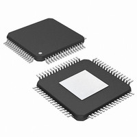
PIC24FJ256DA206-I/MR Microchip Technology, PIC24FJ256DA206-I/MR Datasheet - Page 85

PIC24FJ256DA206-I/MR
Manufacturer Part Number
PIC24FJ256DA206-I/MR
Description
MCU PIC 16BIT FLASH 256K 64VQFN
Manufacturer
Microchip Technology
Series
PIC® 24Fr
Specifications of PIC24FJ256DA206-I/MR
Program Memory Type
FLASH
Program Memory Size
256KB (85.5K x 24)
Package / Case
64-VFQFN, Exposed Pad
Core Processor
PIC
Core Size
16-Bit
Speed
32MHz
Connectivity
I²C, IrDA, SPI, UART/USART, USB OTG
Peripherals
Brown-out Detect/Reset, GFX, LVD, POR, PWM, WDT
Number Of I /o
52
Ram Size
96K x 8
Voltage - Supply (vcc/vdd)
2.2 V ~ 3.6 V
Data Converters
A/D 16x10b
Oscillator Type
Internal
Operating Temperature
-40°C ~ 85°C
Processor Series
PIC24FJ
Core
PIC
Data Bus Width
16 bit
Data Ram Size
96 KB
Interface Type
UART, SPI, USB, I2C, RS-485, RS-232
Maximum Clock Frequency
32 MHz
Number Of Programmable I/os
23
Number Of Timers
5
Operating Supply Voltage
3.6 V
Maximum Operating Temperature
+ 85 C
Mounting Style
SMD/SMT
3rd Party Development Tools
52713-733, 52714-737, 53276-922, EWDSPIC
Development Tools By Supplier
PG164130, DV164035, DV244005, DV164005, AC164127-4, AC164127-6, AC164139, DM240001, DM240312, DV164039
Minimum Operating Temperature
- 40 C
Lead Free Status / RoHS Status
Lead free / RoHS Compliant
Eeprom Size
-
Lead Free Status / Rohs Status
Lead free / RoHS Compliant
- Current page: 85 of 408
- Download datasheet (4Mb)
EXAMPLE 5-2:
EXAMPLE 5-3:
EXAMPLE 5-4:
2010 Microchip Technology Inc.
// C example using MPLAB C30
//Set up pointer to the first memory location to be written
; Set up NVMCON for row programming operations
; Set up a pointer to the first program memory location to be written
; program memory selected, and writes enabled
; Perform the TBLWT instructions to write the latches
; 0th_program_word
; 1st_program_word
;
; 63rd_program_word
2nd_program_word
unsigned long progAddr = 0xXXXXXX;
unsigned int offset;
TBLPAG = progAddr>>16;
offset = progAddr & 0xFFFF;
__builtin_tblwtl(offset, 0x0000);
NVMCON = 0x4042;
asm("DISI #5");
__builtin_write_NVM();
MOV
MOV
MOV
MOV
MOV
MOV
MOV
TBLWTL W2, [W0]
TBLWTH W3, [W0++]
MOV
MOV
TBLWTL W2, [W0]
TBLWTH W3, [W0++]
MOV
MOV
TBLWTL W2, [W0]
TBLWTH W3, [W0++]
•
•
•
MOV
MOV
TBLWTL W2, [W0]
TBLWTH W3, [W0]
DISI
MOV.B
MOV
MOV.B
MOV
BSET
NOP
NOP
BTSC
BRA
#0x4001, W0
W0, NVMCON
#0x0000, W0
W0, TBLPAG
#0x6000, W0
#LOW_WORD_0, W2
#HIGH_BYTE_0, W3
#LOW_WORD_1, W2
#HIGH_BYTE_1, W3
#LOW_WORD_2, W2
#HIGH_BYTE_2, W3
#LOW_WORD_63, W2
#HIGH_BYTE_63, W3
#5
#0x55, W0
W0, NVMKEY
W1, NVMKEY
NVMCON, #WR
NVMCON, #15
$-2
#0xAA, W1
ERASING A PROGRAM MEMORY BLOCK (‘C’ LANGUAGE CODE)
LOADING THE WRITE BUFFERS
INITIATING A PROGRAMMING SEQUENCE
PIC24FJ256DA210 FAMILY
; Block all interrupts with priority <7
; for next 5 instructions
; Write the 0x55 key
;
; Write the 0xAA key
; Start the programming sequence
; Required delays
; and wait for it to be
; completed
// Address of row to write
// Initialize PM Page Boundary SFR
// Initialize lower word of address
// Set base address of erase block
// with dummy latch write
// Initialize NVMCON
// Block all interrupts with priority <7
// for next 5 instructions
// check function to perform unlock
// sequence and set WR
;
; Initialize NVMCON
;
; Initialize PM Page Boundary SFR
; An example program memory address
;
;
; Write PM low word into program latch
; Write PM high byte into program latch
;
;
; Write PM low word into program latch
; Write PM high byte into program latch
;
;
; Write PM low word into program latch
; Write PM high byte into program latch
;
;
; Write PM low word into program latch
; Write PM high byte into program latch
DS39969B-page 85
Related parts for PIC24FJ256DA206-I/MR
Image
Part Number
Description
Manufacturer
Datasheet
Request
R

Part Number:
Description:
Manufacturer:
Microchip Technology Inc.
Datasheet:

Part Number:
Description:
Manufacturer:
Microchip Technology Inc.
Datasheet:

Part Number:
Description:
Manufacturer:
Microchip Technology Inc.
Datasheet:

Part Number:
Description:
Manufacturer:
Microchip Technology Inc.
Datasheet:

Part Number:
Description:
Manufacturer:
Microchip Technology Inc.
Datasheet:

Part Number:
Description:
Manufacturer:
Microchip Technology Inc.
Datasheet:

Part Number:
Description:
Manufacturer:
Microchip Technology Inc.
Datasheet:

Part Number:
Description:
Manufacturer:
Microchip Technology Inc.
Datasheet:


