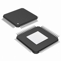
PIC24FJ256DA206-I/MR Microchip Technology, PIC24FJ256DA206-I/MR Datasheet - Page 226

PIC24FJ256DA206-I/MR
Manufacturer Part Number
PIC24FJ256DA206-I/MR
Description
MCU PIC 16BIT FLASH 256K 64VQFN
Manufacturer
Microchip Technology
Series
PIC® 24Fr
Specifications of PIC24FJ256DA206-I/MR
Program Memory Type
FLASH
Program Memory Size
256KB (85.5K x 24)
Package / Case
64-VFQFN, Exposed Pad
Core Processor
PIC
Core Size
16-Bit
Speed
32MHz
Connectivity
I²C, IrDA, SPI, UART/USART, USB OTG
Peripherals
Brown-out Detect/Reset, GFX, LVD, POR, PWM, WDT
Number Of I /o
52
Ram Size
96K x 8
Voltage - Supply (vcc/vdd)
2.2 V ~ 3.6 V
Data Converters
A/D 16x10b
Oscillator Type
Internal
Operating Temperature
-40°C ~ 85°C
Processor Series
PIC24FJ
Core
PIC
Data Bus Width
16 bit
Data Ram Size
96 KB
Interface Type
UART, SPI, USB, I2C, RS-485, RS-232
Maximum Clock Frequency
32 MHz
Number Of Programmable I/os
23
Number Of Timers
5
Operating Supply Voltage
3.6 V
Maximum Operating Temperature
+ 85 C
Mounting Style
SMD/SMT
3rd Party Development Tools
52713-733, 52714-737, 53276-922, EWDSPIC
Development Tools By Supplier
PG164130, DV164035, DV244005, DV164005, AC164127-4, AC164127-6, AC164139, DM240001, DM240312, DV164039
Minimum Operating Temperature
- 40 C
Lead Free Status / RoHS Status
Lead free / RoHS Compliant
Eeprom Size
-
Lead Free Status / Rohs Status
Lead free / RoHS Compliant
- Current page: 226 of 408
- Download datasheet (4Mb)
PIC24FJ256DA210 FAMILY
REGISTER 16-1:
DS39969B-page 226
bit 15
bit 7
Legend:
R = Readable bit
-n = Value at POR
bit 15
bit 14
bit 13
bit 12
bit 11
bit 10
bit 9
bit 8
bit 7
bit 6
I2CEN
GCEN
R/W-0
R/W-0
I2CEN: I2Cx Enable bit
1 = Enables the I2Cx module and configures the SDAx and SCLx pins as serial port pins
0 = Disables the I2Cx module. All I
Unimplemented: Read as ‘0’
I2CSIDL: Stop in Idle Mode bit
1 = Discontinues module operation when device enters an Idle mode
0 = Continues module operation in Idle mode
SCLREL: SCLx Release Control bit (when operating as I
1 = Releases SCLx clock
0 = Holds SCLx clock low (clock stretch)
If STREN = 1:
Bit is R/W (i.e., software may write ‘0’ to initiate stretch and write ‘1’ to release clock). Hardware is clear
at the beginning of slave transmission. Hardware is clear at the end of slave reception.
If STREN = 0:
Bit is R/S (i.e., software may only write ‘1’ to release clock). Hardware clear at beginning of slave
transmission.
IPMIEN: Intelligent Platform Management Interface (IPMI) Enable bit
1 = IPMI Support mode is enabled; all addresses are Acknowledged
0 = IPMI mode is disabled
A10M: 10-Bit Slave Addressing bit
1 = I2CxADD is a 10-bit slave address
0 = I2CxADD is a 7-bit slave address
DISSLW: Disable Slew Rate Control bit
1 = Slew rate control disabled
0 = Slew rate control enabled
SMEN: SMBus Input Levels bit
1 = Enables I/O pin thresholds compliant with SMBus specifications
0 = Disables the SMBus input thresholds
GCEN: General Call Enable bit (when operating as I
1 = Enables interrupt when a general call address is received in the I2CxRSR (module is enabled for
0 = General call address disabled
STREN: SCLx Clock Stretch Enable bit (when operating as I
Used in conjunction with the SCLREL bit.
1 = Enables software or receive clock stretching
0 = Disables software or receive clock stretching
STREN
R/W-0
reception)
U-0
—
I2CxCON: I2Cx CONTROL REGISTER
HC = Hardware Clearable bit
W = Writable bit
‘1’ = Bit is set
I2CSIDL
ACKDT
R/W-0
R/W-0
R/W-1, HC
R/W-0, HC
SCLREL
ACKEN
2
C™ pins are controlled by port functions
U = Unimplemented bit, read as ‘0’
‘0’ = Bit is cleared
R/W-0, HC
IPMIEN
R/W-0
RCEN
2
C slave)
2
C slave)
R/W-0, HC
2
C slave)
R/W-0
A10M
PEN
2010 Microchip Technology Inc.
x = Bit is unknown
R/W-0, HC
DISSLW
R/W-0
RSEN
R/W-0, HC
SMEN
R/W-0
SEN
bit 8
bit 0
Related parts for PIC24FJ256DA206-I/MR
Image
Part Number
Description
Manufacturer
Datasheet
Request
R

Part Number:
Description:
Manufacturer:
Microchip Technology Inc.
Datasheet:

Part Number:
Description:
Manufacturer:
Microchip Technology Inc.
Datasheet:

Part Number:
Description:
Manufacturer:
Microchip Technology Inc.
Datasheet:

Part Number:
Description:
Manufacturer:
Microchip Technology Inc.
Datasheet:

Part Number:
Description:
Manufacturer:
Microchip Technology Inc.
Datasheet:

Part Number:
Description:
Manufacturer:
Microchip Technology Inc.
Datasheet:

Part Number:
Description:
Manufacturer:
Microchip Technology Inc.
Datasheet:

Part Number:
Description:
Manufacturer:
Microchip Technology Inc.
Datasheet:


