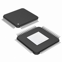
PIC24FJ256DA206-I/MR Microchip Technology, PIC24FJ256DA206-I/MR Datasheet - Page 96

PIC24FJ256DA206-I/MR
Manufacturer Part Number
PIC24FJ256DA206-I/MR
Description
MCU PIC 16BIT FLASH 256K 64VQFN
Manufacturer
Microchip Technology
Series
PIC® 24Fr
Specifications of PIC24FJ256DA206-I/MR
Program Memory Type
FLASH
Program Memory Size
256KB (85.5K x 24)
Package / Case
64-VFQFN, Exposed Pad
Core Processor
PIC
Core Size
16-Bit
Speed
32MHz
Connectivity
I²C, IrDA, SPI, UART/USART, USB OTG
Peripherals
Brown-out Detect/Reset, GFX, LVD, POR, PWM, WDT
Number Of I /o
52
Ram Size
96K x 8
Voltage - Supply (vcc/vdd)
2.2 V ~ 3.6 V
Data Converters
A/D 16x10b
Oscillator Type
Internal
Operating Temperature
-40°C ~ 85°C
Processor Series
PIC24FJ
Core
PIC
Data Bus Width
16 bit
Data Ram Size
96 KB
Interface Type
UART, SPI, USB, I2C, RS-485, RS-232
Maximum Clock Frequency
32 MHz
Number Of Programmable I/os
23
Number Of Timers
5
Operating Supply Voltage
3.6 V
Maximum Operating Temperature
+ 85 C
Mounting Style
SMD/SMT
3rd Party Development Tools
52713-733, 52714-737, 53276-922, EWDSPIC
Development Tools By Supplier
PG164130, DV164035, DV244005, DV164005, AC164127-4, AC164127-6, AC164139, DM240001, DM240312, DV164039
Minimum Operating Temperature
- 40 C
Lead Free Status / RoHS Status
Lead free / RoHS Compliant
Eeprom Size
-
Lead Free Status / Rohs Status
Lead free / RoHS Compliant
- Current page: 96 of 408
- Download datasheet (4Mb)
PIC24FJ256DA210 FAMILY
TABLE 7-2:
7.3
The PIC24FJ256DA210 family of devices implements
a total of 40 registers for the interrupt controller:
• INTCON1
• INTCON2
• IFS0 through IFS6
• IEC0 through IEC6
• IPC0 through IPC25 (except IPC14, IPC17 and
• INTTREG
Global interrupt control functions are controlled from
INTCON1 and INTCON2. INTCON1 contains the Inter-
rupt Nesting Disable (NSTDIS) bit, as well as the
control and status flags for the processor trap sources.
The INTCON2 register controls the external interrupt
request signal behavior and the use of the Alternate
Interrupt Vector Table (AIVT).
The IFSx registers maintain all of the interrupt request
flags. Each source of interrupt has a status bit, which is
set by the respective peripherals or an external signal
and is cleared via software.
The IECx registers maintain all of the interrupt enable
bits. These control bits are used to individually enable
interrupts from the peripherals or external signals.
DS39969B-page 96
Timer1
Timer2
Timer3
Timer4
Timer5
UART1 Error
UART1 Receiver
UART1 Transmitter
UART2 Error
UART2 Receiver
UART2 Transmitter
UART3 Error
UART3 Receiver
UART3 Transmitter
UART4 Error
UART4 Receiver
UART4 Transmitter
USB Interrupt
Note 1:
IPC24)
Interrupt Control and Status
Registers
Interrupt Source
Not available in 64-pin devices (PIC24FJXXXDAX06).
IMPLEMENTED INTERRUPT VECTORS (CONTINUED)
Number
Vector
27
28
65
11
12
66
30
31
81
82
83
87
88
89
86
3
7
8
0000BAh
Address
00001Ah
00004Ah
00004Ch
00002Ah
00002Ch
0000B6h
0000B8h
0000C2h
0000C4h
0000C6h
0000C0h
000022h
000024h
000096h
000098h
000050h
000052h
IVT
Address
00014Ah
00014Ch
00012Ah
00012Ch
0001B6h
0001B8h
0001BAh
0001C2h
0001C4h
0001C6h
0001C0h
00011Ah
000122h
000124h
000196h
000198h
000150h
000152h
The IPCx registers are used to set the interrupt priority
level for each source of interrupt. Each user interrupt
source can be assigned to one of eight priority levels.
The INTTREG register contains the associated
interrupt vector number and the new CPU interrupt
priority level, which are latched into the Vector
Number (VECNUM<6:0>) and the Interrupt Level
(ILR<3:0>) bit fields in the INTTREG register. The
new interrupt priority level is the priority of the
pending interrupt.
The interrupt sources are assigned to the IFSx, IECx
and IPCx registers in the order of their vector numbers,
as shown in Table 7-2. For example, the INT0 (External
Interrupt 0) is shown as having a vector number and a
natural order priority of 0. Thus, the INT0IF status bit is
found in IFS0<0>, the INT0IE enable bit in IEC0<0>
and the INT0IP<2:0> priority bits in the first position of
IPC0 (IPC0<2:0>).
Although they are not specifically part of the interrupt
control hardware, two of the CPU Control registers con-
tain bits that control interrupt functionality. The ALU
STATUS register (SR) contains the IPL<2:0> bits
(SR<7:5>). These indicate the current CPU interrupt
priority level. The user can change the current CPU
priority level by writing to the IPL bits.
AIVT
IFS1<12>
IFS0<12>
IFS1<14>
IFS1<15>
IFS1<11>
IFS0<11>
IFS0<3>
IFS0<7>
IFS0<8>
IFS4<1>
IFS4<2>
IFS5<1>
IFS5<2>
IFS5<3>
IFS5<7>
IFS5<8>
IFS5<9>
IFS5<6>
Flag
Interrupt Bit Locations
2010 Microchip Technology Inc.
IEC1<11>
IEC1<12>
IEC0<11>
IEC0<12>
IEC1<14>
IEC1<15>
IEC0<3>
IEC0<7>
IEC0<8>
IEC4<1>
IEC4<2>
IEC5<1>
IEC5<2>
IEC5<3>
IEC5<7>
IEC5<8>
IEC5<9>
IEC5<6>
Enable
IPC20<14:12>
IPC21<14:12>
IPC0<14:12>
IPC1<14:12>
IPC6<14:12>
IPC2<14:12>
IPC16<10:8>
IPC7<14:12>
IPC20<10:8>
IPC21<10:8>
IPC16<6:4>
IPC7<10:8>
IPC20<6:4>
IPC22<2:0>
IPC22<6:4>
IPC2<2:0>
IPC7<2:0>
IPC3<2:0>
Priority
Related parts for PIC24FJ256DA206-I/MR
Image
Part Number
Description
Manufacturer
Datasheet
Request
R

Part Number:
Description:
Manufacturer:
Microchip Technology Inc.
Datasheet:

Part Number:
Description:
Manufacturer:
Microchip Technology Inc.
Datasheet:

Part Number:
Description:
Manufacturer:
Microchip Technology Inc.
Datasheet:

Part Number:
Description:
Manufacturer:
Microchip Technology Inc.
Datasheet:

Part Number:
Description:
Manufacturer:
Microchip Technology Inc.
Datasheet:

Part Number:
Description:
Manufacturer:
Microchip Technology Inc.
Datasheet:

Part Number:
Description:
Manufacturer:
Microchip Technology Inc.
Datasheet:

Part Number:
Description:
Manufacturer:
Microchip Technology Inc.
Datasheet:


