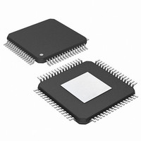
PIC24FJ256DA206-I/MR Microchip Technology, PIC24FJ256DA206-I/MR Datasheet - Page 150

PIC24FJ256DA206-I/MR
Manufacturer Part Number
PIC24FJ256DA206-I/MR
Description
MCU PIC 16BIT FLASH 256K 64VQFN
Manufacturer
Microchip Technology
Series
PIC® 24Fr
Specifications of PIC24FJ256DA206-I/MR
Program Memory Type
FLASH
Program Memory Size
256KB (85.5K x 24)
Package / Case
64-VFQFN, Exposed Pad
Core Processor
PIC
Core Size
16-Bit
Speed
32MHz
Connectivity
I²C, IrDA, SPI, UART/USART, USB OTG
Peripherals
Brown-out Detect/Reset, GFX, LVD, POR, PWM, WDT
Number Of I /o
52
Ram Size
96K x 8
Voltage - Supply (vcc/vdd)
2.2 V ~ 3.6 V
Data Converters
A/D 16x10b
Oscillator Type
Internal
Operating Temperature
-40°C ~ 85°C
Processor Series
PIC24FJ
Core
PIC
Data Bus Width
16 bit
Data Ram Size
96 KB
Interface Type
UART, SPI, USB, I2C, RS-485, RS-232
Maximum Clock Frequency
32 MHz
Number Of Programmable I/os
23
Number Of Timers
5
Operating Supply Voltage
3.6 V
Maximum Operating Temperature
+ 85 C
Mounting Style
SMD/SMT
3rd Party Development Tools
52713-733, 52714-737, 53276-922, EWDSPIC
Development Tools By Supplier
PG164130, DV164035, DV244005, DV164005, AC164127-4, AC164127-6, AC164139, DM240001, DM240312, DV164039
Minimum Operating Temperature
- 40 C
Lead Free Status / RoHS Status
Lead free / RoHS Compliant
Eeprom Size
-
Lead Free Status / Rohs Status
Lead free / RoHS Compliant
- Current page: 150 of 408
- Download datasheet (4Mb)
PIC24FJ256DA210 FAMILY
FIGURE 8-2:
8.5.1
The system clock is generated from the 96 MHz branch
using a configurable postscaler/divider to generate a
range of frequencies for the system clock multiplexer.
The output of the multiplexer is further passed through
a fixed divide-by-3 divider and the final output is used
TABLE 8-2:
DS39969B-page 150
Note 1:
Input from
POSC
Input from
FRC
4 MHz or
8 MHz
These options are not compatible with USB operation. They may be used whenever the PLL branch is
selected and the USB module is disabled.
SYSTEM CLOCK GENERATION
FNOSC<2:0>
SYSTEM CLOCK OPTIONS FOR 96 MHz PLL BLOCK
MCU Clock Division
96 MHz PLL
(CPDIV<1:0>)
96 MHz PLL BLOCK
96 MHz
None (00)
PLL
2 (01)
4 (10)
8 (11)
4 MHz Branch
÷ 5
÷ 4
÷ 3
÷12
÷ 8
÷ 6
÷ 2
÷ 1
96 MHz Branch
PLLDIV<2:0>
111
110
101
100
011
010
001
000
Graphics Clock
Option 1
G1CLKSEL
as the system clock. Figure 8-2 shows this logic in the
system clock sub-block. Since the source is a 96 MHz
signal, the possible system clock frequencies are listed
in Table 8-2. The available system clock options are
always the same, regardless of the setting of the
PLLDIV Configuration bits.
48 MHz Branch
0
1
÷ 2
÷ 8
÷ 4
÷ 2
÷ 1
Graphics Clock
System Clock
USB Clock
CPDIV<1:0>
(Instruction Rate in MIPS)
System Clock Frequency
÷ 2
11
10
01
00
GCLKDIV<6:0>
32 MHz (16)
8 MHz (4)
4 MHz (2)
÷ 64
÷ 63
...
÷ 17.50
÷ 17.00
...
÷ 1.25
÷ 1
16 MHz (8)
Graphics Clock
Option 2
2010 Microchip Technology Inc.
127
126
...
65
64
...
1
0
÷ 3
.
.
.
(1)
(1)
48 MHz Clock
for USB Module
PLL Output for
System Clock
Clock Output for
Display Interface
(DISPCLK)
Clock Output
for Graphics
Controller
Module (G1CLK)
Related parts for PIC24FJ256DA206-I/MR
Image
Part Number
Description
Manufacturer
Datasheet
Request
R

Part Number:
Description:
Manufacturer:
Microchip Technology Inc.
Datasheet:

Part Number:
Description:
Manufacturer:
Microchip Technology Inc.
Datasheet:

Part Number:
Description:
Manufacturer:
Microchip Technology Inc.
Datasheet:

Part Number:
Description:
Manufacturer:
Microchip Technology Inc.
Datasheet:

Part Number:
Description:
Manufacturer:
Microchip Technology Inc.
Datasheet:

Part Number:
Description:
Manufacturer:
Microchip Technology Inc.
Datasheet:

Part Number:
Description:
Manufacturer:
Microchip Technology Inc.
Datasheet:

Part Number:
Description:
Manufacturer:
Microchip Technology Inc.
Datasheet:


