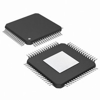
PIC24FJ256DA206-I/MR Microchip Technology, PIC24FJ256DA206-I/MR Datasheet - Page 319

PIC24FJ256DA206-I/MR
Manufacturer Part Number
PIC24FJ256DA206-I/MR
Description
MCU PIC 16BIT FLASH 256K 64VQFN
Manufacturer
Microchip Technology
Series
PIC® 24Fr
Specifications of PIC24FJ256DA206-I/MR
Program Memory Type
FLASH
Program Memory Size
256KB (85.5K x 24)
Package / Case
64-VFQFN, Exposed Pad
Core Processor
PIC
Core Size
16-Bit
Speed
32MHz
Connectivity
I²C, IrDA, SPI, UART/USART, USB OTG
Peripherals
Brown-out Detect/Reset, GFX, LVD, POR, PWM, WDT
Number Of I /o
52
Ram Size
96K x 8
Voltage - Supply (vcc/vdd)
2.2 V ~ 3.6 V
Data Converters
A/D 16x10b
Oscillator Type
Internal
Operating Temperature
-40°C ~ 85°C
Processor Series
PIC24FJ
Core
PIC
Data Bus Width
16 bit
Data Ram Size
96 KB
Interface Type
UART, SPI, USB, I2C, RS-485, RS-232
Maximum Clock Frequency
32 MHz
Number Of Programmable I/os
23
Number Of Timers
5
Operating Supply Voltage
3.6 V
Maximum Operating Temperature
+ 85 C
Mounting Style
SMD/SMT
3rd Party Development Tools
52713-733, 52714-737, 53276-922, EWDSPIC
Development Tools By Supplier
PG164130, DV164035, DV244005, DV164005, AC164127-4, AC164127-6, AC164139, DM240001, DM240312, DV164039
Minimum Operating Temperature
- 40 C
Lead Free Status / RoHS Status
Lead free / RoHS Compliant
Eeprom Size
-
Lead Free Status / Rohs Status
Lead free / RoHS Compliant
- Current page: 319 of 408
- Download datasheet (4Mb)
REGISTER 22-25: G1CLUT: COLOR LOOK-UP TABLE CONTROL REGISTER
2010 Microchip Technology Inc.
bit 15
bit 7
Legend:
R = Readable bit
-n = Value at POR
bit 15
bit 14
bit 13-10
bit 9
bit 8
bit 7-0
CLUTADR7
CLUTEN
R/W-0
R/W-0
CLUTEN: Color Look-up Table Enable Control bit
1 = Color look-up table is enabled
0 = Color look-up table is disabled
CLUTBUSY: Color Look-up Table Busy Status bit
1 = A CLUT entry read/write access is being executed
0 = No CLUT entry read/write access is being executed
Unimplemented: Read as ‘0’
CLUTTRD: Color Look-up Table Read Trigger bit
Enabling this bit will trigger a read to the CLUT location determined by the CLUTADR bits
(G1CLUT<7:0>) with CLUTRWEN enabled.
1 = CLUT read trigger is enabled (must be cleared in software after reading data in the G1CLUTRD
0 = CLUT read trigger is disabled
CLUTRWEN: Color Look-up Table Read/Write Enable Control bit
This bit must be set when reading or modifying entries on the CLUT and it must also be cleared when
CLUT is used by the display controller.
1 = Color look-up table read/write enabled; display controller cannot access the CLUT
0 = Color look-up table read/write disabled; display controller can access the CLUT
CLUTADR<7:0>: Color Look-up Table Memory Address bits
CLUTBUSY
CLUTADR6
R-0, HSC
R/W-0
register)
HSC = Hardware Settable/Clearable bit
W = Writable bit
‘1’ = Bit is set
CLUTADR5 CLUTADR4 CLUTADR3 CLUTADR2 CLUTADR1
R/W-0
U-0
—
PIC24FJ256DA210 FAMILY
R/W-0
U-0
—
U = Unimplemented bit, read as ‘0’
‘0’ = Bit is cleared
R/W-0
U-0
—
R/W-0
U-0
—
x = Bit is unknown
CLUTTRD
R/W-0
R/W-0
DS39969B-page 319
CLUTRWEN
CLUTADR0
R/W-0
R/W-0
bit 8
bit 0
Related parts for PIC24FJ256DA206-I/MR
Image
Part Number
Description
Manufacturer
Datasheet
Request
R

Part Number:
Description:
Manufacturer:
Microchip Technology Inc.
Datasheet:

Part Number:
Description:
Manufacturer:
Microchip Technology Inc.
Datasheet:

Part Number:
Description:
Manufacturer:
Microchip Technology Inc.
Datasheet:

Part Number:
Description:
Manufacturer:
Microchip Technology Inc.
Datasheet:

Part Number:
Description:
Manufacturer:
Microchip Technology Inc.
Datasheet:

Part Number:
Description:
Manufacturer:
Microchip Technology Inc.
Datasheet:

Part Number:
Description:
Manufacturer:
Microchip Technology Inc.
Datasheet:

Part Number:
Description:
Manufacturer:
Microchip Technology Inc.
Datasheet:


