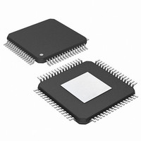
PIC24FJ256DA206-I/MR Microchip Technology, PIC24FJ256DA206-I/MR Datasheet - Page 45

PIC24FJ256DA206-I/MR
Manufacturer Part Number
PIC24FJ256DA206-I/MR
Description
MCU PIC 16BIT FLASH 256K 64VQFN
Manufacturer
Microchip Technology
Series
PIC® 24Fr
Specifications of PIC24FJ256DA206-I/MR
Program Memory Type
FLASH
Program Memory Size
256KB (85.5K x 24)
Package / Case
64-VFQFN, Exposed Pad
Core Processor
PIC
Core Size
16-Bit
Speed
32MHz
Connectivity
I²C, IrDA, SPI, UART/USART, USB OTG
Peripherals
Brown-out Detect/Reset, GFX, LVD, POR, PWM, WDT
Number Of I /o
52
Ram Size
96K x 8
Voltage - Supply (vcc/vdd)
2.2 V ~ 3.6 V
Data Converters
A/D 16x10b
Oscillator Type
Internal
Operating Temperature
-40°C ~ 85°C
Processor Series
PIC24FJ
Core
PIC
Data Bus Width
16 bit
Data Ram Size
96 KB
Interface Type
UART, SPI, USB, I2C, RS-485, RS-232
Maximum Clock Frequency
32 MHz
Number Of Programmable I/os
23
Number Of Timers
5
Operating Supply Voltage
3.6 V
Maximum Operating Temperature
+ 85 C
Mounting Style
SMD/SMT
3rd Party Development Tools
52713-733, 52714-737, 53276-922, EWDSPIC
Development Tools By Supplier
PG164130, DV164035, DV244005, DV164005, AC164127-4, AC164127-6, AC164139, DM240001, DM240312, DV164039
Minimum Operating Temperature
- 40 C
Lead Free Status / RoHS Status
Lead free / RoHS Compliant
Eeprom Size
-
Lead Free Status / Rohs Status
Lead free / RoHS Compliant
- Current page: 45 of 408
- Download datasheet (4Mb)
4.0
As Harvard architecture devices, PIC24F micro-
controllers feature separate program and data memory
spaces and busses. This architecture also allows direct
access of program memory from the data space during
code execution.
4.1
The
PIC24FJ256DA210 family devices is 4M instructions.
The space is addressable by a 24-bit value derived
FIGURE 4-1:
2010 Microchip Technology Inc.
program
Note:
MEMORY ORGANIZATION
Program Memory Space
Memory areas are not shown to scale.
address
PROGRAM SPACE MEMORY MAP FOR PIC24FJ256DA210 FAMILY DEVICES
memory
space
PIC24FJ128DAXXX
Device Config Registers
Alternate Vector Table
Interrupt Vector Table
Flash Config Words
(44K instructions)
Program Memory
GOTO Instruction
Unimplemented
Reset Address
User Flash
DEVID (2)
Reserved
Reserved
Reserved
of
Read ‘0’
PIC24FJ256DA210 FAMILY
the
from either the 23-bit Program Counter (PC) during pro-
gram execution, or from table operation or data space
remapping, as described in Section 4.3 “Interfacing
Program and Data Memory Spaces”.
User access to the program memory space is restricted
to the lower half of the address range (000000h to
7FFFFFh). The exception is the use of TBLRD/TBLWT
operations, which use TBLPAG<7> to permit access to
the Configuration bits and Device ID sections of the
configuration memory space.
Memory maps for the PIC24FJ256DA210 family of
devices are shown in Figure 4-1.
Device Config Registers
PIC24FJ256DAXXX
Alternate Vector Table
Interrupt Vector Table
Flash Config Words
Program Memory
(87K instructions)
GOTO Instruction
Unimplemented
Reset Address
User Flash
DEVID (2)
Reserved
Reserved
Reserved
Read ‘0’
000000h
000002h
000004h
0000FEh
000100h
000104h
0001FEh
000200h
0157FEh
015800h
02ABFEh
02AC00h
7FFFFEh
800000h
F7FFFEh
F80000h
F8000Eh
F80010h
FEFFFEh
FF0000h
FFFFFEh
DS39969B-page 45
Related parts for PIC24FJ256DA206-I/MR
Image
Part Number
Description
Manufacturer
Datasheet
Request
R

Part Number:
Description:
Manufacturer:
Microchip Technology Inc.
Datasheet:

Part Number:
Description:
Manufacturer:
Microchip Technology Inc.
Datasheet:

Part Number:
Description:
Manufacturer:
Microchip Technology Inc.
Datasheet:

Part Number:
Description:
Manufacturer:
Microchip Technology Inc.
Datasheet:

Part Number:
Description:
Manufacturer:
Microchip Technology Inc.
Datasheet:

Part Number:
Description:
Manufacturer:
Microchip Technology Inc.
Datasheet:

Part Number:
Description:
Manufacturer:
Microchip Technology Inc.
Datasheet:

Part Number:
Description:
Manufacturer:
Microchip Technology Inc.
Datasheet:


