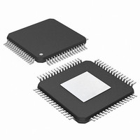
PIC24FJ256DA206-I/MR Microchip Technology, PIC24FJ256DA206-I/MR Datasheet - Page 25

PIC24FJ256DA206-I/MR
Manufacturer Part Number
PIC24FJ256DA206-I/MR
Description
MCU PIC 16BIT FLASH 256K 64VQFN
Manufacturer
Microchip Technology
Series
PIC® 24Fr
Specifications of PIC24FJ256DA206-I/MR
Program Memory Type
FLASH
Program Memory Size
256KB (85.5K x 24)
Package / Case
64-VFQFN, Exposed Pad
Core Processor
PIC
Core Size
16-Bit
Speed
32MHz
Connectivity
I²C, IrDA, SPI, UART/USART, USB OTG
Peripherals
Brown-out Detect/Reset, GFX, LVD, POR, PWM, WDT
Number Of I /o
52
Ram Size
96K x 8
Voltage - Supply (vcc/vdd)
2.2 V ~ 3.6 V
Data Converters
A/D 16x10b
Oscillator Type
Internal
Operating Temperature
-40°C ~ 85°C
Processor Series
PIC24FJ
Core
PIC
Data Bus Width
16 bit
Data Ram Size
96 KB
Interface Type
UART, SPI, USB, I2C, RS-485, RS-232
Maximum Clock Frequency
32 MHz
Number Of Programmable I/os
23
Number Of Timers
5
Operating Supply Voltage
3.6 V
Maximum Operating Temperature
+ 85 C
Mounting Style
SMD/SMT
3rd Party Development Tools
52713-733, 52714-737, 53276-922, EWDSPIC
Development Tools By Supplier
PG164130, DV164035, DV244005, DV164005, AC164127-4, AC164127-6, AC164139, DM240001, DM240312, DV164039
Minimum Operating Temperature
- 40 C
Lead Free Status / RoHS Status
Lead free / RoHS Compliant
Eeprom Size
-
Lead Free Status / Rohs Status
Lead free / RoHS Compliant
- Current page: 25 of 408
- Download datasheet (4Mb)
TABLE 1-3:
2010 Microchip Technology Inc.
PGEC1
PGED1
PGEC2
PGED2
PGEC3
PGED3
PMA0
PMA1
PMA2
PMA3
PMA4
PMA5
PMA6
PMA7
PMA8
PMA9
PMA10
PMA11
PMA12
PMA13
PMA14
PMA15
PMA16
PMA17
PMA18
PMA19
PMA20
PMA21
PMA22
PMACK1
PMACK2
PMALL
PMALH
PMALU
PMBE0
PMBE1
PMCS1
PMCS2
Legend:
Note 1:
Function
2:
3:
4:
TTL = TTL input buffer
ANA = Analog level input/output
The alternate EPMP pins are selected when the ALTPMP (CW3<12>) bit is programmed to ‘0’.
The PMSC2 signal will replace the PMA15 signal on the 15-pin PMA when CSF<1:0> = 01 or 10.
The PMCS1 signal will replace the PMA14 signal on the 14-pin PMA when CSF<1:0> = 10.
The alternate V
TQFP/QFN
64-Pin
15
16
17
18
12
11
—
—
—
—
—
—
—
—
—
—
—
—
—
—
—
—
—
—
—
—
—
—
—
—
—
—
—
—
—
—
—
—
PIC24FJ256DA210 FAMILY PINOUT DESCRIPTIONS (CONTINUED)
Pin Number
REF
12, 60
59, 11
100-Pin
11,59
10,40
40,10
60,12
71
70
66,9
TQFP
66
pins selected when the ALTVREF (CW1<5>) bit is programmed to ‘0’.
(3)
24
25
26
27
20
21
44
43
14
29
28
50
49
42
41
35
34
71
70
95
92
19
77
69
44
43
14
78
67
(2)
(1)
,18
(1)
,9,
(1)
(1)
(1)
(1)
(1)
(1)
F2, G11
G10, F4
D11
C11
F4,G10
G11,F2
E11,E1
E3,K6
K6,E3
121-Pin
E11
BGA
L10
C11
D11
A10
E10
L11
G2
K1
K2
H1
H2
K7
F3
K3
C4
B5
K7
B9
E8
L1
J3
L8
L2
L7
J7
J5
L5
L8
F3
(2)
(3)
(1)
,E1,
,G1
(1)
(1)
(1)
(1)
(1)
(1)
(1)
PIC24FJ256DA210 FAMILY
I/O
I/O
I/O
I/O
I/O
I/O
I/O
I/O
I/O
I/O
O
O
O
O
O
O
O
O
O
O
O
O
O
O
O
O
O
O
O
O
O
O
O
O
O
O
O
I
I
ST/TTL Parallel Master Port Acknowledge Input 1.
ST/TTL Parallel Master Port Acknowledge Input 2.
ST/TTL Parallel Master Port Chip Select Strobe 1.
Buffer
Input
ST
ST
ST
ST
ST
ST
ST
ST
—
—
—
—
—
—
—
—
—
—
—
—
—
—
—
—
—
—
—
—
—
—
—
—
—
—
—
ST = Schmitt Trigger input buffer
I
2
C™ = I
In-Circuit Debugger/Emulator/ICSP™ Programming Clock 1.
In-Circuit Debugger/Emulator/ICSP Programming Data 1.
In-Circuit Debugger/Emulator/ICSP Programming Clock 2.
In-Circuit Debugger/Emulator/ICSP Programming Data 2.
In-Circuit Debugger/Emulator/ICSP Programming Clock 3.
In-Circuit Debugger/Emulator/ICSP Programming Data 3.
Parallel Master Port Address bit 0 Input (Buffered Slave
modes) and Output (Master modes).
Parallel Master Port Address Bit 1 Input (Buffered Slave
modes) and Output (Master modes).
Parallel Master Port Address bits<22:2>.
Parallel Master Port Lower Address Latch Strobe.
Parallel Master Port Higher Address Latch Strobe.
Parallel Master Port Upper Address Latch Strobe.
Parallel Master Port Byte Enable Strobe 0.
Parallel Master Port Byte Enable Strobe 1.
Parallel Master Port Chip Select Strobe 2.
2
C/SMBus input buffer
Description
DS39969B-page 25
Related parts for PIC24FJ256DA206-I/MR
Image
Part Number
Description
Manufacturer
Datasheet
Request
R

Part Number:
Description:
Manufacturer:
Microchip Technology Inc.
Datasheet:

Part Number:
Description:
Manufacturer:
Microchip Technology Inc.
Datasheet:

Part Number:
Description:
Manufacturer:
Microchip Technology Inc.
Datasheet:

Part Number:
Description:
Manufacturer:
Microchip Technology Inc.
Datasheet:

Part Number:
Description:
Manufacturer:
Microchip Technology Inc.
Datasheet:

Part Number:
Description:
Manufacturer:
Microchip Technology Inc.
Datasheet:

Part Number:
Description:
Manufacturer:
Microchip Technology Inc.
Datasheet:

Part Number:
Description:
Manufacturer:
Microchip Technology Inc.
Datasheet:


