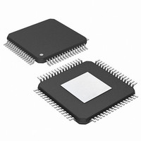
PIC24FJ256DA206-I/MR Microchip Technology, PIC24FJ256DA206-I/MR Datasheet - Page 318

PIC24FJ256DA206-I/MR
Manufacturer Part Number
PIC24FJ256DA206-I/MR
Description
MCU PIC 16BIT FLASH 256K 64VQFN
Manufacturer
Microchip Technology
Series
PIC® 24Fr
Specifications of PIC24FJ256DA206-I/MR
Program Memory Type
FLASH
Program Memory Size
256KB (85.5K x 24)
Package / Case
64-VFQFN, Exposed Pad
Core Processor
PIC
Core Size
16-Bit
Speed
32MHz
Connectivity
I²C, IrDA, SPI, UART/USART, USB OTG
Peripherals
Brown-out Detect/Reset, GFX, LVD, POR, PWM, WDT
Number Of I /o
52
Ram Size
96K x 8
Voltage - Supply (vcc/vdd)
2.2 V ~ 3.6 V
Data Converters
A/D 16x10b
Oscillator Type
Internal
Operating Temperature
-40°C ~ 85°C
Processor Series
PIC24FJ
Core
PIC
Data Bus Width
16 bit
Data Ram Size
96 KB
Interface Type
UART, SPI, USB, I2C, RS-485, RS-232
Maximum Clock Frequency
32 MHz
Number Of Programmable I/os
23
Number Of Timers
5
Operating Supply Voltage
3.6 V
Maximum Operating Temperature
+ 85 C
Mounting Style
SMD/SMT
3rd Party Development Tools
52713-733, 52714-737, 53276-922, EWDSPIC
Development Tools By Supplier
PG164130, DV164035, DV244005, DV164005, AC164127-4, AC164127-6, AC164139, DM240001, DM240312, DV164039
Minimum Operating Temperature
- 40 C
Lead Free Status / RoHS Status
Lead free / RoHS Compliant
Eeprom Size
-
Lead Free Status / Rohs Status
Lead free / RoHS Compliant
- Current page: 318 of 408
- Download datasheet (4Mb)
PIC24FJ256DA210 FAMILY
REGISTER 22-23: G1VSYNC: VERTICAL SYNCHRONIZATION CONTROL REGISTER
REGISTER 22-24: G1DBLCON: DISPLAY BLANKING CONTROL REGISTER
DS39969B-page 318
bit 15
bit 7
Legend:
R = Readable bit
-n = Value at POR
bit 15-8
bit 7-0
bit 15
bit 7
Legend:
R = Readable bit
-n = Value at POR
bit 15-8
bit 7-0
VSLEN7
VENST7
HENST7
VSST7
R/W-0
R/W-0
R/W-0
R/W-0
VSLEN<7:0>: V
The DPVSOE bit (G1CON3<1>) must be set for the V
VSST<7:0>: V
This is the number of lines from the start of vertical blanking to the start of V
VENST<7:0>: Vertical Blanking Start to First Displayed Line Configuration bits (in lines)
This is the number of lines from the start of vertical blanking to the first displayed line of a frame.
HENST<7:0>: Horizontal Blanking Start to First Displayed Pixel Configuration bits (in DISPCLKs)
This is the number of GCLK cycles from the start of horizontal blanking to the first displayed pixel of
each displayed line.
VSLEN6
VENST6
HENST6
VSST6
R/W-0
R/W-0
R/W-0
R/W-0
SYNC
W = Writable bit
‘1’ = Bit is set
W = Writable bit
‘1’ = Bit is set
SYNC
VSLEN5
VSST5
HENST5
VENST5
R/W-0
R/W-0
R/W-0
R/W-0
Start Delay Configuration bits (in lines)
Pulse-Width Configuration bits (in lines)
VSLEN4
VSST4
R/W-0
R/W-0
VENST4
HENST4
R/W-0
R/W-0
U = Unimplemented bit, read as ‘0’
‘0’ = Bit is cleared
U = Unimplemented bit, read as ‘0’
‘0’ = Bit is cleared
VSLEN3
VSST3
R/W-0
R/W-0
HENST3
VENST3
R/W-0
R/W-0
SYNC
signal to toggle; minimum value is 1.
VSLEN2
VSST2
R/W-0
R/W-0
HENST2
VENST2
R/W-0
R/W-0
x = Bit is unknown
2010 Microchip Technology Inc.
x = Bit is unknown
VSLEN1
SYNC
VSST1
R/W-0
R/W-0
VENST1
HENST1
R/W-0
R/W-0
active.
VSLEN0
VENST0
HENST0
VSST0
R/W-0
R/W-0
R/W-0
R/W-0
bit 8
bit 0
bit 8
bit 0
Related parts for PIC24FJ256DA206-I/MR
Image
Part Number
Description
Manufacturer
Datasheet
Request
R

Part Number:
Description:
Manufacturer:
Microchip Technology Inc.
Datasheet:

Part Number:
Description:
Manufacturer:
Microchip Technology Inc.
Datasheet:

Part Number:
Description:
Manufacturer:
Microchip Technology Inc.
Datasheet:

Part Number:
Description:
Manufacturer:
Microchip Technology Inc.
Datasheet:

Part Number:
Description:
Manufacturer:
Microchip Technology Inc.
Datasheet:

Part Number:
Description:
Manufacturer:
Microchip Technology Inc.
Datasheet:

Part Number:
Description:
Manufacturer:
Microchip Technology Inc.
Datasheet:

Part Number:
Description:
Manufacturer:
Microchip Technology Inc.
Datasheet:


