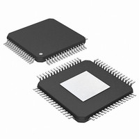
PIC24FJ256DA206-I/MR Microchip Technology, PIC24FJ256DA206-I/MR Datasheet - Page 327

PIC24FJ256DA206-I/MR
Manufacturer Part Number
PIC24FJ256DA206-I/MR
Description
MCU PIC 16BIT FLASH 256K 64VQFN
Manufacturer
Microchip Technology
Series
PIC® 24Fr
Specifications of PIC24FJ256DA206-I/MR
Program Memory Type
FLASH
Program Memory Size
256KB (85.5K x 24)
Package / Case
64-VFQFN, Exposed Pad
Core Processor
PIC
Core Size
16-Bit
Speed
32MHz
Connectivity
I²C, IrDA, SPI, UART/USART, USB OTG
Peripherals
Brown-out Detect/Reset, GFX, LVD, POR, PWM, WDT
Number Of I /o
52
Ram Size
96K x 8
Voltage - Supply (vcc/vdd)
2.2 V ~ 3.6 V
Data Converters
A/D 16x10b
Oscillator Type
Internal
Operating Temperature
-40°C ~ 85°C
Processor Series
PIC24FJ
Core
PIC
Data Bus Width
16 bit
Data Ram Size
96 KB
Interface Type
UART, SPI, USB, I2C, RS-485, RS-232
Maximum Clock Frequency
32 MHz
Number Of Programmable I/os
23
Number Of Timers
5
Operating Supply Voltage
3.6 V
Maximum Operating Temperature
+ 85 C
Mounting Style
SMD/SMT
3rd Party Development Tools
52713-733, 52714-737, 53276-922, EWDSPIC
Development Tools By Supplier
PG164130, DV164035, DV244005, DV164005, AC164127-4, AC164127-6, AC164139, DM240001, DM240312, DV164039
Minimum Operating Temperature
- 40 C
Lead Free Status / RoHS Status
Lead free / RoHS Compliant
Eeprom Size
-
Lead Free Status / Rohs Status
Lead free / RoHS Compliant
- Current page: 327 of 408
- Download datasheet (4Mb)
REGISTER 23-1:
2010 Microchip Technology Inc.
bit 15
bit 7
Legend:
R = Readable bit
-n = Value at POR
bit 15
bit 14
bit 13
bit 12-10
bit 9-8
bit 7-5
bit 4-3
bit 2
bit 1
bit 0
Note 1:
ADON
SSRC2
R/W-0
R/W-0
(1)
The values of the ADC1BUFx registers will not retain their values once the ADON bit is cleared. Read out
the conversion values from the buffer before disabling the module.
ADON: A/D Operating Mode bit
1 = A/D Converter module is operating
0 = A/D Converter is off
Unimplemented: Read as ‘0’
ADSIDL: Stop in Idle Mode bit
1 = Discontinue module operation when device enters Idle mode
0 = Continue module operation in Idle mode
Unimplemented: Read as ‘0’
FORM<1:0>: Data Output Format bits
11 = Signed fractional (sddd dddd dd00 0000)
10 = Fractional (dddd dddd dd00 0000)
01 = Signed integer (ssss sssd dddd dddd)
00 = Integer (0000 00dd dddd dddd)
SSRC<2:0>: Conversion Trigger Source Select bits
111 = Internal counter ends sampling and starts conversion (auto-convert)
110 = CTMU event ends sampling and starts conversion
101 = Reserved
100 = Timer5 compare ends sampling and starts conversion
011 = Reserved
010 = Timer3 compare ends sampling and starts conversion
001 = Active transition on INT0 pin ends sampling and starts conversion
000 = Clearing SAMP bit ends sampling and starts conversion
Unimplemented: Read as ‘0’
ASAM: A/D Sample Auto-Start bit
1 = Sampling begins immediately after the last conversion completes. The SAMP bit is auto-set.
0 = Sampling begins when the SAMP bit is set
SAMP: A/D Sample Enable bit
1 = A/D sample/hold amplifier is sampling input
0 = A/D sample/hold amplifier is holding
DONE: A/D Conversion Status bit
1 = A/D conversion is done
0 = A/D conversion is NOT done
SSRC1
R/W-0
U-0
—
AD1CON1: A/D CONTROL REGISTER 1
HSC = Hardware Settable/Clearable bit
W = Writable bit
‘1’ = Bit is set
ADSIDL
SSRC0
R/W-0
R/W-0
(1)
PIC24FJ256DA210 FAMILY
U-0
U-0
—
—
U = Unimplemented bit, read as ‘0’
‘0’ = Bit is cleared
U-0
U-0
—
—
R/W-0
ASAM
U-0
—
x = Bit is unknown
R-0, HSC
FORM1
SAMP
R/W-0
DS39969B-page 327
R-0, HSC
FORM0
R/W-0
DONE
bit 8
bit 0
Related parts for PIC24FJ256DA206-I/MR
Image
Part Number
Description
Manufacturer
Datasheet
Request
R

Part Number:
Description:
Manufacturer:
Microchip Technology Inc.
Datasheet:

Part Number:
Description:
Manufacturer:
Microchip Technology Inc.
Datasheet:

Part Number:
Description:
Manufacturer:
Microchip Technology Inc.
Datasheet:

Part Number:
Description:
Manufacturer:
Microchip Technology Inc.
Datasheet:

Part Number:
Description:
Manufacturer:
Microchip Technology Inc.
Datasheet:

Part Number:
Description:
Manufacturer:
Microchip Technology Inc.
Datasheet:

Part Number:
Description:
Manufacturer:
Microchip Technology Inc.
Datasheet:

Part Number:
Description:
Manufacturer:
Microchip Technology Inc.
Datasheet:


