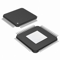
PIC24FJ256DA206-I/MR Microchip Technology, PIC24FJ256DA206-I/MR Datasheet - Page 158

PIC24FJ256DA206-I/MR
Manufacturer Part Number
PIC24FJ256DA206-I/MR
Description
MCU PIC 16BIT FLASH 256K 64VQFN
Manufacturer
Microchip Technology
Series
PIC® 24Fr
Specifications of PIC24FJ256DA206-I/MR
Program Memory Type
FLASH
Program Memory Size
256KB (85.5K x 24)
Package / Case
64-VFQFN, Exposed Pad
Core Processor
PIC
Core Size
16-Bit
Speed
32MHz
Connectivity
I²C, IrDA, SPI, UART/USART, USB OTG
Peripherals
Brown-out Detect/Reset, GFX, LVD, POR, PWM, WDT
Number Of I /o
52
Ram Size
96K x 8
Voltage - Supply (vcc/vdd)
2.2 V ~ 3.6 V
Data Converters
A/D 16x10b
Oscillator Type
Internal
Operating Temperature
-40°C ~ 85°C
Processor Series
PIC24FJ
Core
PIC
Data Bus Width
16 bit
Data Ram Size
96 KB
Interface Type
UART, SPI, USB, I2C, RS-485, RS-232
Maximum Clock Frequency
32 MHz
Number Of Programmable I/os
23
Number Of Timers
5
Operating Supply Voltage
3.6 V
Maximum Operating Temperature
+ 85 C
Mounting Style
SMD/SMT
3rd Party Development Tools
52713-733, 52714-737, 53276-922, EWDSPIC
Development Tools By Supplier
PG164130, DV164035, DV244005, DV164005, AC164127-4, AC164127-6, AC164139, DM240001, DM240312, DV164039
Minimum Operating Temperature
- 40 C
Lead Free Status / RoHS Status
Lead free / RoHS Compliant
Eeprom Size
-
Lead Free Status / Rohs Status
Lead free / RoHS Compliant
- Current page: 158 of 408
- Download datasheet (4Mb)
corresponding pin to act as an open-drain output.
PIC24FJ256DA210 FAMILY
10.1.1
One instruction cycle is required between a port direction
change or port write operation and a read operation of
the same port. Typically, this instruction would be a NOP.
10.1.2
In addition to the PORT, LAT and TRIS registers for data
control, each port pin can also be individually configured
for either a digital or open-drain output. This is controlled
by the Open-Drain Control register, ODCx, associated
with each port. Setting any of the bits configures the
The open-drain feature allows the generation of
outputs higher than V
digital only pins by using external pull-up resistors. The
maximum open-drain voltage allowed is the same as
the maximum V
10.1.3
The input buffers of the RG2 and RG3 pins are by
default, tri-stated. To use these pins as input pins, the
UTRDIS bit (U1CNFG2<0>) should be set which
enables the input buffers on these pins.
TABLE 10-1:
TABLE 10-2:
DS39969B-page 158
Analog Input
Analog Output
Digital Input
Digital Output
PORTA
PORTB<15:0>
PORTC
PORTD<7:6>
PORTE
PORTF<0>
PORTG<9:6, 3:2>
PORTA
PORTC
PORTD
PORTE
PORTF
PORTG
Note 1:
Pin Function
(1)
(1)
(1)
(1)
(1)
(1)
(1)
(1)
(1)
<10:9, 7:6>
<15:14, 5:0>
<13:12, 8:7, 5:1>
<9>
<8:0>
<15:12, 4>
<3:1>
<15:8, 5:0>
<15:12, 1:0>
Not all of the pins of these PORTS are implemented in 64-pin devices (PIC24FJXXXDAX06); refer to the
device pinout diagrams for the details.
I/O PORT WRITE/READ TIMING
OPEN-DRAIN CONFIGURATION
CONFIGURING D+ AND D- PINS
(RG2 AND RG3)
Port or Pin
IH
specification.
CONFIGURING ANALOG/DIGITAL FUNCTION OF AN I/O PIN
INPUT VOLTAGE LEVELS FOR PORT OR PIN TOLERATED DESCRIPTION INPUT
DD
ANSx Setting
(e.g., 5V) on any desired
1
1
0
0
TRISx Setting
Tolerated Input
1
1
1
0
5.5V
V
DD
10.2
The ANSx and TRISx registers control the operation of
the pins with analog function. Each port pin with analog
function is associated with one of the ANS bits (see
Register 10-1 through Register 10-7), which decides if
the pin function should be analog or digital. Refer to
Table 10-1 for detailed behavior of the pin for different
ANSx and TRISx bit settings.
When reading the PORT register, all pins configured as
analog input channels will read as cleared (a low level).
10.2.1
The voltage tolerance of pins used as device inputs is
dependent on the pin’s input function. Pins that are used
as digital only inputs are able to handle DC voltages of up
to 5.5V, a level typical for digital logic circuits. In contrast,
pins that also have analog input functions of any kind can
only tolerate voltages up to V
beyond V
Table 10-2 summarizes the input capabilities. Refer to
Section 30.1 “DC Characteristics” for more details.
It is recommended to keep ANSx = 1.
It is recommended to keep ANSx = 1.
Firmware must wait at least one instruction cycle
after configuring a pin as a digital input before a valid
input value can be read.
Make sure to disable the analog output function on
the pin if any is present.
Configuring Analog Port Pins
(ANSEL)
DD
ANALOG INPUT PINS AND
VOLTAGE CONSIDERATIONS
on these pins should always be avoided.
Only V
Tolerates input levels above V
for most standard logic.
DD
Comments
input levels are tolerated.
2010 Microchip Technology Inc.
Description
DD
. Voltage excursions
DD
, useful
Related parts for PIC24FJ256DA206-I/MR
Image
Part Number
Description
Manufacturer
Datasheet
Request
R

Part Number:
Description:
Manufacturer:
Microchip Technology Inc.
Datasheet:

Part Number:
Description:
Manufacturer:
Microchip Technology Inc.
Datasheet:

Part Number:
Description:
Manufacturer:
Microchip Technology Inc.
Datasheet:

Part Number:
Description:
Manufacturer:
Microchip Technology Inc.
Datasheet:

Part Number:
Description:
Manufacturer:
Microchip Technology Inc.
Datasheet:

Part Number:
Description:
Manufacturer:
Microchip Technology Inc.
Datasheet:

Part Number:
Description:
Manufacturer:
Microchip Technology Inc.
Datasheet:

Part Number:
Description:
Manufacturer:
Microchip Technology Inc.
Datasheet:


