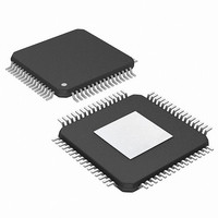
PIC24FJ256DA206-I/MR Microchip Technology, PIC24FJ256DA206-I/MR Datasheet - Page 202

PIC24FJ256DA206-I/MR
Manufacturer Part Number
PIC24FJ256DA206-I/MR
Description
MCU PIC 16BIT FLASH 256K 64VQFN
Manufacturer
Microchip Technology
Series
PIC® 24Fr
Specifications of PIC24FJ256DA206-I/MR
Program Memory Type
FLASH
Program Memory Size
256KB (85.5K x 24)
Package / Case
64-VFQFN, Exposed Pad
Core Processor
PIC
Core Size
16-Bit
Speed
32MHz
Connectivity
I²C, IrDA, SPI, UART/USART, USB OTG
Peripherals
Brown-out Detect/Reset, GFX, LVD, POR, PWM, WDT
Number Of I /o
52
Ram Size
96K x 8
Voltage - Supply (vcc/vdd)
2.2 V ~ 3.6 V
Data Converters
A/D 16x10b
Oscillator Type
Internal
Operating Temperature
-40°C ~ 85°C
Processor Series
PIC24FJ
Core
PIC
Data Bus Width
16 bit
Data Ram Size
96 KB
Interface Type
UART, SPI, USB, I2C, RS-485, RS-232
Maximum Clock Frequency
32 MHz
Number Of Programmable I/os
23
Number Of Timers
5
Operating Supply Voltage
3.6 V
Maximum Operating Temperature
+ 85 C
Mounting Style
SMD/SMT
3rd Party Development Tools
52713-733, 52714-737, 53276-922, EWDSPIC
Development Tools By Supplier
PG164130, DV164035, DV244005, DV164005, AC164127-4, AC164127-6, AC164139, DM240001, DM240312, DV164039
Minimum Operating Temperature
- 40 C
Lead Free Status / RoHS Status
Lead free / RoHS Compliant
Eeprom Size
-
Lead Free Status / Rohs Status
Lead free / RoHS Compliant
- Current page: 202 of 408
- Download datasheet (4Mb)
PIC24FJ256DA210 FAMILY
FIGURE 14-1:
14.2
In Compare mode (Figure 14-1), the output compare
module can be configured for single-shot or continuous
pulse generation. It can also repeatedly toggle an
output pin on each timer event.
To set up the module for compare operations:
1.
2.
DS39969B-page 202
Trigger and
Sync Sources
OC Clock
Sources
Configure the OCx output for one of the
available Peripheral Pin Select pins.
Calculate the required values for the OCxR and
(for Double Compare modes) OCxRS Duty Cycle
registers:
a)
b)
c)
Note 1: The OCx outputs must be assigned to an available RPn pin before use. See Section 10.4 “Peripheral Pin
Compare Operations
Determine the instruction clock cycle time.
Take into account the frequency of the
external clock to the timer source (if one is
used) and the timer prescaler settings.
Calculate time to the rising edge of the
output pulse relative to the timer start value
(0000h).
Calculate the time to the falling edge of the
pulse based on the desired pulse width and
the time to the rising edge of the pulse.
2: The OCFA/OCFB fault inputs must be assigned to an available RPn/RPIn pin before use. See Section 10.4
Select (PPS)” for more information.
“Peripheral Pin Select (PPS)” for more information.
TRIGMODE
SYNCSELx
TRIGSTAT
OCTSELx
OCTRIG
Trigger and
Sync Logic
OUTPUT COMPARE BLOCK DIAGRAM (16-BIT MODE)
Select
Clock
Match Event
Reset
Increment
Reset
OCxR and
Comparator
Comparator
DCB<1:0>
OCxCON1
OCxCON2
OCxTMR
OCxRS
3.
4.
5.
6.
7.
8.
Match Event
Match Event
Write the rising edge value to OCxR and the
falling edge value to OCxRS.
Set the Timer Period register, PRy, to a value
equal to or greater than the value in OCxRS.
Set the OCM<2:0> bits for the appropriate
compare operation (= 0xx).
For Trigger mode operations, set OCTRIG to
enable Trigger mode. Set or clear TRIGMODE to
configure trigger operation and TRIGSTAT to
select a hardware or software trigger. For
Synchronous mode, clear OCTRIG.
Set the SYNCSEL<4:0> bits to configure the
trigger or synchronization source. If free-running
timer operation is required, set the SYNCSEL
bits to ‘00000’ (no sync/trigger source).
Select
OCTSEL<2:0> bits. If necessary, set the TON
bits for the selected timer, which enables the
compare time base to count. Synchronous
mode operation starts as soon as the time base
is enabled; Trigger mode operation starts after a
trigger source event occurs.
the
OC Output and
Fault Logic
OCx Interrupt
time
OCMx
OCINV
OCTRIS
FLTOUT
FLTTRIEN
FLTMD
ENFLT<2:0>
OCFLT<2:0>
DCB<1:0>
2010 Microchip Technology Inc.
base
source
OCFA/OCFB
OCx Pin
with
(1)
the
(2)
Related parts for PIC24FJ256DA206-I/MR
Image
Part Number
Description
Manufacturer
Datasheet
Request
R

Part Number:
Description:
Manufacturer:
Microchip Technology Inc.
Datasheet:

Part Number:
Description:
Manufacturer:
Microchip Technology Inc.
Datasheet:

Part Number:
Description:
Manufacturer:
Microchip Technology Inc.
Datasheet:

Part Number:
Description:
Manufacturer:
Microchip Technology Inc.
Datasheet:

Part Number:
Description:
Manufacturer:
Microchip Technology Inc.
Datasheet:

Part Number:
Description:
Manufacturer:
Microchip Technology Inc.
Datasheet:

Part Number:
Description:
Manufacturer:
Microchip Technology Inc.
Datasheet:

Part Number:
Description:
Manufacturer:
Microchip Technology Inc.
Datasheet:


