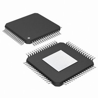
PIC24FJ256DA206-I/MR Microchip Technology, PIC24FJ256DA206-I/MR Datasheet - Page 76

PIC24FJ256DA206-I/MR
Manufacturer Part Number
PIC24FJ256DA206-I/MR
Description
MCU PIC 16BIT FLASH 256K 64VQFN
Manufacturer
Microchip Technology
Series
PIC® 24Fr
Specifications of PIC24FJ256DA206-I/MR
Program Memory Type
FLASH
Program Memory Size
256KB (85.5K x 24)
Package / Case
64-VFQFN, Exposed Pad
Core Processor
PIC
Core Size
16-Bit
Speed
32MHz
Connectivity
I²C, IrDA, SPI, UART/USART, USB OTG
Peripherals
Brown-out Detect/Reset, GFX, LVD, POR, PWM, WDT
Number Of I /o
52
Ram Size
96K x 8
Voltage - Supply (vcc/vdd)
2.2 V ~ 3.6 V
Data Converters
A/D 16x10b
Oscillator Type
Internal
Operating Temperature
-40°C ~ 85°C
Processor Series
PIC24FJ
Core
PIC
Data Bus Width
16 bit
Data Ram Size
96 KB
Interface Type
UART, SPI, USB, I2C, RS-485, RS-232
Maximum Clock Frequency
32 MHz
Number Of Programmable I/os
23
Number Of Timers
5
Operating Supply Voltage
3.6 V
Maximum Operating Temperature
+ 85 C
Mounting Style
SMD/SMT
3rd Party Development Tools
52713-733, 52714-737, 53276-922, EWDSPIC
Development Tools By Supplier
PG164130, DV164035, DV244005, DV164005, AC164127-4, AC164127-6, AC164139, DM240001, DM240312, DV164039
Minimum Operating Temperature
- 40 C
Lead Free Status / RoHS Status
Lead free / RoHS Compliant
Eeprom Size
-
Lead Free Status / Rohs Status
Lead free / RoHS Compliant
- Current page: 76 of 408
- Download datasheet (4Mb)
PIC24FJ256DA210 FAMILY
TABLE 4-36:
FIGURE 4-8:
DS39969B-page 76
Instruction Access
(Code Execution)
TBLRD/TBLWT
(Byte/Word Read/Write)
Program Space Visibility
(Block Remap/Read)
Note 1:
Note 1: DSRPAG<8> acts as word select. DSRPAG<9> should always be ‘1’ to map program memory to data memory.
Access Type
2:
Program Counter
Table Operations
Program Space Visibility
(Remapping)
2: The instructions, TBLRDH/TBLWTH/TBLRDL/TBLWTL, decide if the higher or lower word of program memory is
Data EA<15> is always ‘1’ in this case, but is not used in calculating the program space address. Bit 15 of
the address is DSRPAG<0>.
program memory is read. When DSRPAG<8> is ‘0’, the lower word is read and when it is ‘1’, the higher
word is read.
DSRPAG<9> is always ‘1’ in this case. DSRPAG<8> decides whether the lower word or higher word of
accessed. TBLRDH/TBLWTH instructions access the higher word and TBLRDL/TBLWTL instructions access the
lower word. Table read operations are permitted in the configuration memory space.
PROGRAM SPACE ADDRESS CONSTRUCTION
DATA ACCESS FROM PROGRAM SPACE ADDRESS GENERATION
(2)
User
User
Configuration
User
(1)
User/Configuration
1-Bit
Access
Space
Space Select
1/0
0
0
TBLPAG
8 Bits
DSRPAG<7:0>
<23>
8 Bits
0
0
0
Select
TBLPAG<7:0>
TBLPAG<7:0>
0xxx xxxx
1xxx xxxx
Program Counter
0xx xxxx xxxx xxxx xxxx xxx0
<22:16>
DSRPAG<7:0>
24 Bits
1
xxxx xxxx
23 Bits
23 Bits
Program Space Address
PC<22:1>
(2)
16 Bits
<15>
15 Bits
EA
EA
xxxx xxxx xxxx xxxx
xxxx xxxx xxxx xxxx
2010 Microchip Technology Inc.
Data EA<15:0>
Data EA<15:0>
xxx xxxx xxxx xxxx
<14:1>
Data EA<14:0>
Byte Select
1/0
1/0
0
(1)
<0>
0
Related parts for PIC24FJ256DA206-I/MR
Image
Part Number
Description
Manufacturer
Datasheet
Request
R

Part Number:
Description:
Manufacturer:
Microchip Technology Inc.
Datasheet:

Part Number:
Description:
Manufacturer:
Microchip Technology Inc.
Datasheet:

Part Number:
Description:
Manufacturer:
Microchip Technology Inc.
Datasheet:

Part Number:
Description:
Manufacturer:
Microchip Technology Inc.
Datasheet:

Part Number:
Description:
Manufacturer:
Microchip Technology Inc.
Datasheet:

Part Number:
Description:
Manufacturer:
Microchip Technology Inc.
Datasheet:

Part Number:
Description:
Manufacturer:
Microchip Technology Inc.
Datasheet:

Part Number:
Description:
Manufacturer:
Microchip Technology Inc.
Datasheet:


