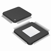
PIC24FJ256DA206-I/MR Microchip Technology, PIC24FJ256DA206-I/MR Datasheet - Page 205

PIC24FJ256DA206-I/MR
Manufacturer Part Number
PIC24FJ256DA206-I/MR
Description
MCU PIC 16BIT FLASH 256K 64VQFN
Manufacturer
Microchip Technology
Series
PIC® 24Fr
Specifications of PIC24FJ256DA206-I/MR
Program Memory Type
FLASH
Program Memory Size
256KB (85.5K x 24)
Package / Case
64-VFQFN, Exposed Pad
Core Processor
PIC
Core Size
16-Bit
Speed
32MHz
Connectivity
I²C, IrDA, SPI, UART/USART, USB OTG
Peripherals
Brown-out Detect/Reset, GFX, LVD, POR, PWM, WDT
Number Of I /o
52
Ram Size
96K x 8
Voltage - Supply (vcc/vdd)
2.2 V ~ 3.6 V
Data Converters
A/D 16x10b
Oscillator Type
Internal
Operating Temperature
-40°C ~ 85°C
Processor Series
PIC24FJ
Core
PIC
Data Bus Width
16 bit
Data Ram Size
96 KB
Interface Type
UART, SPI, USB, I2C, RS-485, RS-232
Maximum Clock Frequency
32 MHz
Number Of Programmable I/os
23
Number Of Timers
5
Operating Supply Voltage
3.6 V
Maximum Operating Temperature
+ 85 C
Mounting Style
SMD/SMT
3rd Party Development Tools
52713-733, 52714-737, 53276-922, EWDSPIC
Development Tools By Supplier
PG164130, DV164035, DV244005, DV164005, AC164127-4, AC164127-6, AC164139, DM240001, DM240312, DV164039
Minimum Operating Temperature
- 40 C
Lead Free Status / RoHS Status
Lead free / RoHS Compliant
Eeprom Size
-
Lead Free Status / Rohs Status
Lead free / RoHS Compliant
- Current page: 205 of 408
- Download datasheet (4Mb)
14.3.2
The PWM duty cycle is specified by writing to the
OCxRS and OCxR registers. The OCxRS and OCxR
registers can be written to at any time, but the duty
cycle value is not latched until a match between PRy
and TMRy occurs (i.e., the period is complete). This
provides a double buffer for the PWM duty cycle and is
essential for glitchless PWM operation.
Some important boundary parameters of the PWM duty
cycle include:
EQUATION 14-2:
EXAMPLE 14-1:
TABLE 14-1:
TABLE 14-2:
2010 Microchip Technology Inc.
Timer Prescaler Ratio
Period Register Value
Resolution (bits)
Note 1:
Timer Prescaler Ratio
Period Register Value
Resolution (bits)
Note 1:
1.
2.
Note 1:
Find the Timer Period register value for a desired PWM frequency of 52.08 kHz, where F
(32 MHz device clock rate) and a Timer2 prescaler setting of 1:1.
Find the maximum resolution of the duty cycle that can be used with a 52.08 kHz frequency and a 32 MHz device
clock rate:
PWM Frequency
PWM Frequency
T
PWM Period = 1/PWM Frequency = 1/52.08 kHz = 19.2 ms
PWM Period = (PR2 + 1) • T
19.2 ms = PR2 + 1) • 62.5 ns • 1
PR2 = 306
PWM Resolution = log
= (log
= 8.3 bits
CY
Based on F
Based on F
PWM DUTY CYCLE
Note 1: Based on F
Based on T
= 2 * T
10
(16 MHz/52.08 kHz)/log
Maximum PWM Resolution (bits) =
EXAMPLE PWM FREQUENCIES AND RESOLUTIONS AT 4 MIPS (F
EXAMPLE PWM FREQUENCIES AND RESOLUTIONS AT 16 MIPS (F
OSC
CALCULATION FOR MAXIMUM PWM RESOLUTION
PWM PERIOD AND DUTY CYCLE CALCULATIONS
CY
CY
CY
= 62.5 ns
= F
= F
= 2 * T
OSC
OSC
10
CY
(F
OSC
30.5 Hz
FFFFh
/2; Doze mode and PLL are disabled.
FFFFh
/2; Doze mode and PLL are disabled.
7.6 Hz
CY
16
16
= F
8
8
CY
; Doze mode and PLL are disabled.
/F
OSC
PWM
• (Timer2 Prescale Value)
10
2) bits
/2; Doze mode and PLL are disabled.
)/log
244 Hz
FFFFh
FFFFh
61 Hz
PIC24FJ256DA210 FAMILY
log
16
16
10
1
1
2) bits
10
(
FPWM • (Timer Prescale Value)
122 Hz
488 Hz
7FFFh
7FFFh
15
15
1
1
• If OCxR, OCxRS, and PRy are all loaded with
• If OCxRS is greater than PRy, the pin will remain
See Example 14-1 for PWM mode timing details.
Table 14-1 and Table 14-2 show example PWM
4 MIPS and 10 MIPS, respectively.
frequencies and resolutions for a device operating at
0000h, the OCx pin will remain low (0% duty
cycle).
high (100% duty cycle).
log
F
CY
10
3.9 kHz
977 Hz
0FFFh
0FFFh
(2)
12
12
1
1
15.6 kHz
(1)
3.9 kHz
03FFh
03FFh
(1)
)
10
10
1
1
bits
OSC
31.3 kHz
125 kHz
007Fh
007Fh
= 8 MHz with PLL
CY
CY
1
7
1
7
DS39969B-page 205
= 4 MHz)
= 16 MHz)
125 kHz
500 kHz
001Fh
001Fh
(1)
1
5
1
5
(1)
Related parts for PIC24FJ256DA206-I/MR
Image
Part Number
Description
Manufacturer
Datasheet
Request
R

Part Number:
Description:
Manufacturer:
Microchip Technology Inc.
Datasheet:

Part Number:
Description:
Manufacturer:
Microchip Technology Inc.
Datasheet:

Part Number:
Description:
Manufacturer:
Microchip Technology Inc.
Datasheet:

Part Number:
Description:
Manufacturer:
Microchip Technology Inc.
Datasheet:

Part Number:
Description:
Manufacturer:
Microchip Technology Inc.
Datasheet:

Part Number:
Description:
Manufacturer:
Microchip Technology Inc.
Datasheet:

Part Number:
Description:
Manufacturer:
Microchip Technology Inc.
Datasheet:

Part Number:
Description:
Manufacturer:
Microchip Technology Inc.
Datasheet:


