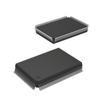
HD64F2636UF20 Renesas Electronics America, HD64F2636UF20 Datasheet - Page 233

HD64F2636UF20
Manufacturer Part Number
HD64F2636UF20
Description
IC H8S MCU FLASH 128K 128QFP
Manufacturer
Renesas Electronics America
Series
H8® H8S/2600r
Specifications of HD64F2636UF20
Core Processor
H8S/2600
Core Size
16-Bit
Speed
20MHz
Connectivity
CAN, SCI, SmartCard
Peripherals
Motor Control PWM, POR, PWM, WDT
Number Of I /o
72
Program Memory Size
128KB (128K x 8)
Program Memory Type
FLASH
Ram Size
4K x 8
Voltage - Supply (vcc/vdd)
4.5 V ~ 5.5 V
Data Converters
A/D 12x10b; D/A 2x8b
Oscillator Type
Internal
Operating Temperature
-20°C ~ 75°C
Package / Case
128-QFP
Lead Free Status / RoHS Status
Contains lead / RoHS non-compliant
Eeprom Size
-
- Current page: 233 of 1512
- Download datasheet (9Mb)
H8S/2639, H8S/2638, H8S/2636,
H8S/2630, H8S/2635 Group
(2) Write after Read
If an external write occurs after an external read while the ICIS0 bit in BCRH is set to 1, an idle
cycle is inserted at the start of the write cycle.
Figure 7-16 shows an example of the operation in this case. In this example, bus cycle A is a read
cycle from ROM with a long output floating time, and bus cycle B is a CPU write cycle. In (a), an
idle cycle is not inserted, and a collision occurs in cycle B between the read data from ROM and
the CPU write data. In (b), an idle cycle is inserted, and a data collision is prevented.
REJ09B0103-0800 Rev. 8.00
May 28, 2010
CS* (area A)
CS* (area B)
Address bus
Note: * The CS signal is generated externally rather than inside the LSI device.
RD
Possibility of overlap between
CS (area B) and RD
φ
(a) Idle cycle not inserted
T
1
Bus cycle A
(ICIS1 = 0)
Figure 7-16 Example of Idle Cycle Operation (2)
T
2
T
3
Bus cycle B
T
1
T
2
CS* (area A)
CS* (area B)
Address bus
RD
φ
T
1
Bus cycle A
(b) Idle cycle inserted
T
(Initial value ICIS1 = 1)
2
T
3
Section 7 Bus Controller
T
I
Bus cycle B
Page 183 of 1458
T
1
T
2
Related parts for HD64F2636UF20
Image
Part Number
Description
Manufacturer
Datasheet
Request
R

Part Number:
Description:
KIT STARTER FOR M16C/29
Manufacturer:
Renesas Electronics America
Datasheet:

Part Number:
Description:
KIT STARTER FOR R8C/2D
Manufacturer:
Renesas Electronics America
Datasheet:

Part Number:
Description:
R0K33062P STARTER KIT
Manufacturer:
Renesas Electronics America
Datasheet:

Part Number:
Description:
KIT STARTER FOR R8C/23 E8A
Manufacturer:
Renesas Electronics America
Datasheet:

Part Number:
Description:
KIT STARTER FOR R8C/25
Manufacturer:
Renesas Electronics America
Datasheet:

Part Number:
Description:
KIT STARTER H8S2456 SHARPE DSPLY
Manufacturer:
Renesas Electronics America
Datasheet:

Part Number:
Description:
KIT STARTER FOR R8C38C
Manufacturer:
Renesas Electronics America
Datasheet:

Part Number:
Description:
KIT STARTER FOR R8C35C
Manufacturer:
Renesas Electronics America
Datasheet:

Part Number:
Description:
KIT STARTER FOR R8CL3AC+LCD APPS
Manufacturer:
Renesas Electronics America
Datasheet:

Part Number:
Description:
KIT STARTER FOR RX610
Manufacturer:
Renesas Electronics America
Datasheet:

Part Number:
Description:
KIT STARTER FOR R32C/118
Manufacturer:
Renesas Electronics America
Datasheet:

Part Number:
Description:
KIT DEV RSK-R8C/26-29
Manufacturer:
Renesas Electronics America
Datasheet:

Part Number:
Description:
KIT STARTER FOR SH7124
Manufacturer:
Renesas Electronics America
Datasheet:

Part Number:
Description:
KIT STARTER FOR H8SX/1622
Manufacturer:
Renesas Electronics America
Datasheet:


