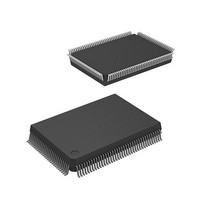
HD64F2636UF20 Renesas Electronics America, HD64F2636UF20 Datasheet - Page 555

HD64F2636UF20
Manufacturer Part Number
HD64F2636UF20
Description
IC H8S MCU FLASH 128K 128QFP
Manufacturer
Renesas Electronics America
Series
H8® H8S/2600r
Specifications of HD64F2636UF20
Core Processor
H8S/2600
Core Size
16-Bit
Speed
20MHz
Connectivity
CAN, SCI, SmartCard
Peripherals
Motor Control PWM, POR, PWM, WDT
Number Of I /o
72
Program Memory Size
128KB (128K x 8)
Program Memory Type
FLASH
Ram Size
4K x 8
Voltage - Supply (vcc/vdd)
4.5 V ~ 5.5 V
Data Converters
A/D 12x10b; D/A 2x8b
Oscillator Type
Internal
Operating Temperature
-20°C ~ 75°C
Package / Case
128-QFP
Lead Free Status / RoHS Status
Contains lead / RoHS non-compliant
Eeprom Size
-
- Current page: 555 of 1512
- Download datasheet (9Mb)
H8S/2639, H8S/2638, H8S/2636,
H8S/2630, H8S/2635 Group
Section 13 Serial Communication Interface (SCI)
Break Detection and Processing (Asynchronous Mode Only): When framing error (FER)
detection is performed, a break can be detected by reading the RxD pin value directly. In a break,
the input from the RxD pin becomes all 0s, and so the FER flag is set, and the parity error flag
(PER) may also be set.
Note that, since the SCI continues the receive operation after receiving a break, even if the FER
flag is cleared to 0, it will be set to 1 again.
Sending a Break (Asynchronous Mode Only): The TxD pin has a dual function as an I/O port
whose direction (input or output) is determined by DR and DDR. This can be used to send a break.
Between serial transmission initialization and setting of the TE bit to 1, the mark state is replaced
by the value of DR (the pin does not function as the TxD pin until the TE bit is set to 1).
Consequently, DDR and DR for the port corresponding to the TxD pin are first set to 1.
To send a break during serial transmission, first clear DR to 0, then clear the TE bit to 0.
When the TE bit is cleared to 0, the transmitter is initialized regardless of the current transmission
state, the TxD pin becomes an I/O port, and 0 is output from the TxD pin.
Receive Error Flags and Transmit Operations (Clocked Synchronous Mode Only):
Transmission cannot be started when a receive error flag (ORER, PER, or FER) is set to 1, even if
the TDRE flag is cleared to 0. Be sure to clear the receive error flags to 0 before starting
transmission.
Note also that receive error flags cannot be cleared to 0 even if the RE bit is cleared to 0.
Receive Data Sampling Timing and Reception Margin in Asynchronous Mode:
In asynchronous mode, the SCI operates on a basic clock with a frequency of 16 times the transfer
rate.
In reception, the SCI samples the falling edge of the start bit using the basic clock, and performs
internal synchronization. Receive data is latched internally at the rising edge of the 8th pulse of the
basic clock. This is illustrated in figure 13-21.
REJ09B0103-0800 Rev. 8.00
Page 505 of 1458
May 28, 2010
Related parts for HD64F2636UF20
Image
Part Number
Description
Manufacturer
Datasheet
Request
R

Part Number:
Description:
KIT STARTER FOR M16C/29
Manufacturer:
Renesas Electronics America
Datasheet:

Part Number:
Description:
KIT STARTER FOR R8C/2D
Manufacturer:
Renesas Electronics America
Datasheet:

Part Number:
Description:
R0K33062P STARTER KIT
Manufacturer:
Renesas Electronics America
Datasheet:

Part Number:
Description:
KIT STARTER FOR R8C/23 E8A
Manufacturer:
Renesas Electronics America
Datasheet:

Part Number:
Description:
KIT STARTER FOR R8C/25
Manufacturer:
Renesas Electronics America
Datasheet:

Part Number:
Description:
KIT STARTER H8S2456 SHARPE DSPLY
Manufacturer:
Renesas Electronics America
Datasheet:

Part Number:
Description:
KIT STARTER FOR R8C38C
Manufacturer:
Renesas Electronics America
Datasheet:

Part Number:
Description:
KIT STARTER FOR R8C35C
Manufacturer:
Renesas Electronics America
Datasheet:

Part Number:
Description:
KIT STARTER FOR R8CL3AC+LCD APPS
Manufacturer:
Renesas Electronics America
Datasheet:

Part Number:
Description:
KIT STARTER FOR RX610
Manufacturer:
Renesas Electronics America
Datasheet:

Part Number:
Description:
KIT STARTER FOR R32C/118
Manufacturer:
Renesas Electronics America
Datasheet:

Part Number:
Description:
KIT DEV RSK-R8C/26-29
Manufacturer:
Renesas Electronics America
Datasheet:

Part Number:
Description:
KIT STARTER FOR SH7124
Manufacturer:
Renesas Electronics America
Datasheet:

Part Number:
Description:
KIT STARTER FOR H8SX/1622
Manufacturer:
Renesas Electronics America
Datasheet:


