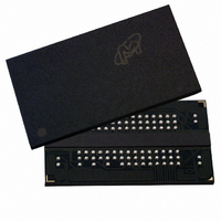
MT47H256M4BT-5E:A TR Micron Technology Inc, MT47H256M4BT-5E:A TR Datasheet - Page 101

MT47H256M4BT-5E:A TR
Manufacturer Part Number
MT47H256M4BT-5E:A TR
Description
IC DDR2 SDRAM 1GBIT 5NS 92FBGA
Manufacturer
Micron Technology Inc
Datasheet
1.MT47H256M4HQ-5EE_TR.pdf
(131 pages)
Specifications of MT47H256M4BT-5E:A TR
Format - Memory
RAM
Memory Type
DDR2 SDRAM
Memory Size
1G (256M x 4)
Speed
5ns
Interface
Parallel
Voltage - Supply
1.7 V ~ 1.9 V
Operating Temperature
0°C ~ 85°C
Package / Case
92-FBGA
Lead Free Status / RoHS Status
Lead free / RoHS Compliant
Other names
557-1206-1
- Current page: 101 of 131
- Download datasheet (10Mb)
Figure 56: Data Output Timing –
WRITE
PDF: 09005aef821ae8bf
1GbDDR2.pdf – Rev. T 02/10 EN
LDQS#/LDQS/UDQ#/UDQS 3
All DQs collectively 4
DQ (first data valid)
DQ (last data valid)
DQS#/DQS or
Notes:
CK#
CK
WRITE bursts are initiated with a WRITE command. DDR2 SDRAM uses WL equal to RL
minus one clock cycle (WL = RL - 1CK) (see READ (page 73)). The starting column and
bank addresses are provided with the WRITE command, and auto precharge is either
enabled or disabled for that access. If auto precharge is enabled, the row being accessed
is precharged at the completion of the burst.
Note:
For the WRITE commands used in the following illustrations, auto precharge is disabled.
During WRITE bursts, the first valid data-in element will be registered on the first rising
edge of DQS following the WRITE command, and subsequent data elements will be reg-
istered on successive edges of DQS. The LOW state on DQS between the WRITE com-
mand and the first rising edge is known as the write preamble; the LOW state on DQS
following the last data-in element is known as the write postamble.
The time between the WRITE command and the first rising DQS edge is WL ±
Subsequent DQS positive rising edges are timed, relative to the associated clock edge,
as ±
T0 1
5.
6. The data valid window is derived for each DQS transition and is
7. DQ8, DQ9, DQ10, D11, DQ12, DQ13, DQ14, or DQ15.
1. READ command with CL = 3, AL = 0 issued at T0.
2.
3. DQ transitioning after DQS transitions define
4. All DQ must transition by
5.
6.
7.
8. I/O balls, when entering or exiting High-Z, are not referenced to a specific voltage level,
t
DQSS.
t
t
DQS skew.
t
skew.
t
t
but to when the device begins to drive or no longer drives, respectively.
QH is derived from
DQSCK is the DQS output window relative to CK and is the long-term component of
AC is the DQ output window relative to CK and is the “long term” component of DQ
LZ (MIN) and
HZ (MAX) and
t
t
AC and
T1
DQSS is specified with a relatively wide range (25% of one clock cycle). All of
t LZ (MIN)
t
AC (MIN) are the first valid signal transitions.
t
t
AC (MAX) are the latest valid signal transitions.
DQSCK
T2
t
HP:
t LZ (MIN)
t RPRE
t
QH =
101
t
DQSQ after DQS transitions, regardless of
t DQSCK 2 (MIN)
T3
t
HP -
T3
T3
T3
T3n
t
Micron Technology, Inc. reserves the right to change products or specifications without notice.
QHS.
t AC 5 (MIN)
T3n
T3n
T3n
T4
T4
1Gb: x4, x8, x16 DDR2 SDRAM
T4
T4
t
DQSQ window.
T4n
T4n
t AC 5 (MAX)
T4n
T4n
T5
T5
t DQSCK 2 (MAX)
T5
T5
T5n
© 2004 Micron Technology, Inc. All rights reserved.
T5n
T5n
T5n
t
QH -
T6
t HZ (MAX)
T6
T6
T6
t HZ (MAX)
t
AC.
t
T6n
DQSQ.
t RPST
T6n
T6n
T6n
T7
t
DQSS.
WRITE
Related parts for MT47H256M4BT-5E:A TR
Image
Part Number
Description
Manufacturer
Datasheet
Request
R

Part Number:
Description:
IC DDR2 SDRAM 1GBIT 92FBGA
Manufacturer:
Micron Technology Inc
Datasheet:

Part Number:
Description:
IC DDR2 SDRAM 1GBIT 3NS 92FBGA
Manufacturer:
Micron Technology Inc
Datasheet:

Part Number:
Description:
IC DDR2 SDRAM 1GBIT 5NS 92FBGA
Manufacturer:
Micron Technology Inc
Datasheet:

Part Number:
Description:
IC SDRAM 64MBIT 133MHZ 54TSOP
Manufacturer:
Micron Technology Inc
Datasheet:

Part Number:
Description:
IC SDRAM 64MBIT 5.5NS 86TSOP
Manufacturer:
Micron Technology Inc
Datasheet:

Part Number:
Description:
IC SDRAM 64MBIT 200MHZ 86TSOP
Manufacturer:
Micron Technology Inc
Datasheet:

Part Number:
Description:
IC SDRAM 64MBIT 133MHZ 54TSOP
Manufacturer:
Micron Technology Inc
Datasheet:

Part Number:
Description:
IC SDRAM 128MBIT 133MHZ 54TSOP
Manufacturer:
Micron Technology Inc
Datasheet:

Part Number:
Description:
IC SDRAM 256MBIT 133MHZ 90VFBGA
Manufacturer:
Micron Technology Inc
Datasheet:

Part Number:
Description:
IC SDRAM 128MBIT 133MHZ 54TSOP
Manufacturer:
Micron Technology Inc
Datasheet:

Part Number:
Description:
IC SDRAM 256MBIT 133MHZ 54TSOP
Manufacturer:
Micron Technology Inc
Datasheet:

Part Number:
Description:
IC DDR SDRAM 512MBIT 6NS 66TSOP
Manufacturer:
Micron Technology Inc
Datasheet:

Part Number:
Description:
IC SDRAM 128MBIT 167MHZ 86TSOP
Manufacturer:
Micron Technology Inc
Datasheet:

Part Number:
Description:
IC SDRAM 128MBIT 143MHZ 86TSOP
Manufacturer:
Micron Technology Inc
Datasheet:

Part Number:
Description:
SDRAM 256M-BIT 1.8V 54-PIN VFBGA
Manufacturer:
Micron Technology Inc
Datasheet:


