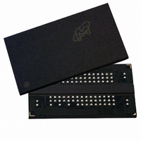
MT47H256M4BT-5E:A TR Micron Technology Inc, MT47H256M4BT-5E:A TR Datasheet - Page 13

MT47H256M4BT-5E:A TR
Manufacturer Part Number
MT47H256M4BT-5E:A TR
Description
IC DDR2 SDRAM 1GBIT 5NS 92FBGA
Manufacturer
Micron Technology Inc
Datasheet
1.MT47H256M4HQ-5EE_TR.pdf
(131 pages)
Specifications of MT47H256M4BT-5E:A TR
Format - Memory
RAM
Memory Type
DDR2 SDRAM
Memory Size
1G (256M x 4)
Speed
5ns
Interface
Parallel
Voltage - Supply
1.7 V ~ 1.9 V
Operating Temperature
0°C ~ 85°C
Package / Case
92-FBGA
Lead Free Status / RoHS Status
Lead free / RoHS Compliant
Other names
557-1206-1
- Current page: 13 of 131
- Download datasheet (10Mb)
Figure 4: 128 Meg x 8 Functional Block Diagram
PDF: 09005aef821ae8bf
1GbDDR2.pdf – Rev. T 02/10 EN
BA0–BA2
A0–A13,
RAS#
CAS#
ODT
WE#
CKE
CK#
CS#
CK
17
Address
register
registers
Mode
Control
logic
17
Refresh
counter
14
10
3
14
address
2
Row-
MUX
14
control
Bank
Column-
logic
counter/
address
latch
decoder
address
Bank 0
latch
row-
and
Bank 1
Bank 2
Bank 3
8
2
Bank 4
16,384
Bank 5
Bank 6
Bank 7
DM mask logic
(16,384 x 256 x 32)
I/O gating
Memory array
Sense amplifers
decoder
Column
8,192
(x32)
256
Bank 0
Bank 1
Bank 2
Bank 3
Bank 4
Bank 5
Bank 6
13
Bank 7
COL0, COL1
CK,CK#
32
32
32
Micron Technology, Inc. reserves the right to change products or specifications without notice.
Read
latch
CK out
drivers
WRITE
CK in
FIFO
and
8
8
8
8
Mask
COL0, COL1
Data
4
32
1Gb: x4, x8, x16 DDR2 SDRAM
MUX
generator
2
2
2
8
8
8
8
2
DQS
registers
Input
Functional Block Diagrams
Data
8
UDQS, UDQS#
LDQS, LDQS#
2
2
2
2
8
8
8
8
CK, CK#
2
8
2
DRVRS
2
DLL
RCVRS
© 2004 Micron Technology, Inc. All rights reserved.
sw1 sw2
sw1 sw2
sw1 sw2
sw1 sw2
R1
R1
R1
R1
R1
R1
ODT control
R2
R2
R2
R2
R2
R2
V
ss
Q
sw3
sw3
sw3
sw3
R3
R3
R3
R3
R3
R3
V
dd
Q
DQ0–DQ7
DQS, DQS#
RDQS#
RDQS
DM
Related parts for MT47H256M4BT-5E:A TR
Image
Part Number
Description
Manufacturer
Datasheet
Request
R

Part Number:
Description:
IC DDR2 SDRAM 1GBIT 92FBGA
Manufacturer:
Micron Technology Inc
Datasheet:

Part Number:
Description:
IC DDR2 SDRAM 1GBIT 3NS 92FBGA
Manufacturer:
Micron Technology Inc
Datasheet:

Part Number:
Description:
IC DDR2 SDRAM 1GBIT 5NS 92FBGA
Manufacturer:
Micron Technology Inc
Datasheet:

Part Number:
Description:
IC SDRAM 64MBIT 133MHZ 54TSOP
Manufacturer:
Micron Technology Inc
Datasheet:

Part Number:
Description:
IC SDRAM 64MBIT 5.5NS 86TSOP
Manufacturer:
Micron Technology Inc
Datasheet:

Part Number:
Description:
IC SDRAM 64MBIT 200MHZ 86TSOP
Manufacturer:
Micron Technology Inc
Datasheet:

Part Number:
Description:
IC SDRAM 64MBIT 133MHZ 54TSOP
Manufacturer:
Micron Technology Inc
Datasheet:

Part Number:
Description:
IC SDRAM 128MBIT 133MHZ 54TSOP
Manufacturer:
Micron Technology Inc
Datasheet:

Part Number:
Description:
IC SDRAM 256MBIT 133MHZ 90VFBGA
Manufacturer:
Micron Technology Inc
Datasheet:

Part Number:
Description:
IC SDRAM 128MBIT 133MHZ 54TSOP
Manufacturer:
Micron Technology Inc
Datasheet:

Part Number:
Description:
IC SDRAM 256MBIT 133MHZ 54TSOP
Manufacturer:
Micron Technology Inc
Datasheet:

Part Number:
Description:
IC DDR SDRAM 512MBIT 6NS 66TSOP
Manufacturer:
Micron Technology Inc
Datasheet:

Part Number:
Description:
IC SDRAM 128MBIT 167MHZ 86TSOP
Manufacturer:
Micron Technology Inc
Datasheet:

Part Number:
Description:
IC SDRAM 128MBIT 143MHZ 86TSOP
Manufacturer:
Micron Technology Inc
Datasheet:

Part Number:
Description:
SDRAM 256M-BIT 1.8V 54-PIN VFBGA
Manufacturer:
Micron Technology Inc
Datasheet:


