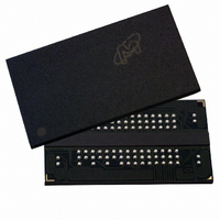
MT47H256M4BT-5E:A TR Micron Technology Inc, MT47H256M4BT-5E:A TR Datasheet - Page 73

MT47H256M4BT-5E:A TR
Manufacturer Part Number
MT47H256M4BT-5E:A TR
Description
IC DDR2 SDRAM 1GBIT 5NS 92FBGA
Manufacturer
Micron Technology Inc
Datasheet
1.MT47H256M4HQ-5EE_TR.pdf
(131 pages)
Specifications of MT47H256M4BT-5E:A TR
Format - Memory
RAM
Memory Type
DDR2 SDRAM
Memory Size
1G (256M x 4)
Speed
5ns
Interface
Parallel
Voltage - Supply
1.7 V ~ 1.9 V
Operating Temperature
0°C ~ 85°C
Package / Case
92-FBGA
Lead Free Status / RoHS Status
Lead free / RoHS Compliant
Other names
557-1206-1
- Current page: 73 of 131
- Download datasheet (10Mb)
NO OPERATION (NOP)
LOAD MODE (LM)
ACTIVATE
READ
WRITE
PDF: 09005aef821ae8bf
1GbDDR2.pdf – Rev. T 02/10 EN
The NO OPERATION (NOP) command is used to instruct the selected DDR2 SDRAM to
perform a NOP (CS# is LOW; RAS#, CAS#, and WE are HIGH). This prevents unwanted
commands from being registered during idle or wait states. Operations already in pro-
gress are not affected.
The mode registers are loaded via bank address and address inputs. The bank address
balls determine which mode register will be programmed. See Mode Register (MR)
(page 74). The LM command can only be issued when all banks are idle, and a subse-
quent executable command cannot be issued until
The ACTIVATE command is used to open (or activate) a row in a particular bank for a
subsequent access. The value on the bank address inputs determines the bank, and the
address inputs select the row. This row remains active (or open) for accesses until a pre-
charge command is issued to that bank. A precharge command must be issued before
opening a different row in the same bank.
The READ command is used to initiate a burst read access to an active row. The value
on the bank address inputs determine the bank, and the address provided on address
inputs A0–Ai (where Ai is the most significant column address bit for a given configura-
tion) selects the starting column location. The value on input A10 determines whether
or not auto precharge is used. If auto precharge is selected, the row being accessed will
be precharged at the end of the read burst; if auto precharge is not selected, the row will
remain open for subsequent accesses.
DDR2 SDRAM also supports the AL feature, which allows a READ or WRITE command
to be issued prior to
command to the internal device by AL clock cycles.
The WRITE command is used to initiate a burst write access to an active row. The value
on the bank select inputs selects the bank, and the address provided on inputs A0–Ai
(where Ai is the most significant column address bit for a given configuration) selects
the starting column location. The value on input A10 determines whether or not auto
precharge is used. If auto precharge is selected, the row being accessed will be pre-
charged at the end of the WRITE burst; if auto precharge is not selected, the row will
remain open for subsequent accesses.
DDR2 SDRAM also supports the AL feature, which allows a READ or WRITE command
to be issued prior to
command to the internal device by AL clock cycles.
Input data appearing on the DQ is written to the memory array subject to the DM input
logic level appearing coincident with the data. If a given DM signal is registered LOW,
the corresponding data will be written to memory; if the DM signal is registered HIGH,
the corresponding data inputs will be ignored, and a WRITE will not be executed to that
byte/column location (see Figure 65 (page 110)).
t
t
RCD (MIN) by delaying the actual registration of the READ/WRITE
RCD (MIN) by delaying the actual registration of the READ/WRITE
73
Micron Technology, Inc. reserves the right to change products or specifications without notice.
1Gb: x4, x8, x16 DDR2 SDRAM
t
MRD is met.
© 2004 Micron Technology, Inc. All rights reserved.
Commands
Related parts for MT47H256M4BT-5E:A TR
Image
Part Number
Description
Manufacturer
Datasheet
Request
R

Part Number:
Description:
IC DDR2 SDRAM 1GBIT 92FBGA
Manufacturer:
Micron Technology Inc
Datasheet:

Part Number:
Description:
IC DDR2 SDRAM 1GBIT 3NS 92FBGA
Manufacturer:
Micron Technology Inc
Datasheet:

Part Number:
Description:
IC DDR2 SDRAM 1GBIT 5NS 92FBGA
Manufacturer:
Micron Technology Inc
Datasheet:

Part Number:
Description:
IC SDRAM 64MBIT 133MHZ 54TSOP
Manufacturer:
Micron Technology Inc
Datasheet:

Part Number:
Description:
IC SDRAM 64MBIT 5.5NS 86TSOP
Manufacturer:
Micron Technology Inc
Datasheet:

Part Number:
Description:
IC SDRAM 64MBIT 200MHZ 86TSOP
Manufacturer:
Micron Technology Inc
Datasheet:

Part Number:
Description:
IC SDRAM 64MBIT 133MHZ 54TSOP
Manufacturer:
Micron Technology Inc
Datasheet:

Part Number:
Description:
IC SDRAM 128MBIT 133MHZ 54TSOP
Manufacturer:
Micron Technology Inc
Datasheet:

Part Number:
Description:
IC SDRAM 256MBIT 133MHZ 90VFBGA
Manufacturer:
Micron Technology Inc
Datasheet:

Part Number:
Description:
IC SDRAM 128MBIT 133MHZ 54TSOP
Manufacturer:
Micron Technology Inc
Datasheet:

Part Number:
Description:
IC SDRAM 256MBIT 133MHZ 54TSOP
Manufacturer:
Micron Technology Inc
Datasheet:

Part Number:
Description:
IC DDR SDRAM 512MBIT 6NS 66TSOP
Manufacturer:
Micron Technology Inc
Datasheet:

Part Number:
Description:
IC SDRAM 128MBIT 167MHZ 86TSOP
Manufacturer:
Micron Technology Inc
Datasheet:

Part Number:
Description:
IC SDRAM 128MBIT 143MHZ 86TSOP
Manufacturer:
Micron Technology Inc
Datasheet:

Part Number:
Description:
SDRAM 256M-BIT 1.8V 54-PIN VFBGA
Manufacturer:
Micron Technology Inc
Datasheet:


