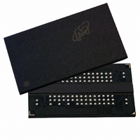
MT47H256M4BT-5E:A TR Micron Technology Inc, MT47H256M4BT-5E:A TR Datasheet - Page 76

MT47H256M4BT-5E:A TR
Manufacturer Part Number
MT47H256M4BT-5E:A TR
Description
IC DDR2 SDRAM 1GBIT 5NS 92FBGA
Manufacturer
Micron Technology Inc
Datasheet
1.MT47H256M4HQ-5EE_TR.pdf
(131 pages)
Specifications of MT47H256M4BT-5E:A TR
Format - Memory
RAM
Memory Type
DDR2 SDRAM
Memory Size
1G (256M x 4)
Speed
5ns
Interface
Parallel
Voltage - Supply
1.7 V ~ 1.9 V
Operating Temperature
0°C ~ 85°C
Package / Case
92-FBGA
Lead Free Status / RoHS Status
Lead free / RoHS Compliant
Other names
557-1206-1
- Current page: 76 of 131
- Download datasheet (10Mb)
Burst Type
Table 40: Burst Definition
Operating Mode
DLL RESET
PDF: 09005aef821ae8bf
1GbDDR2.pdf – Rev. T 02/10 EN
Burst Length
4
8
Starting Column Address
Accesses within a given burst may be programmed to be either sequential or inter-
leaved. The burst type is selected via bit M3, as shown in Figure 35. The ordering of
accesses within a burst is determined by the burst length, the burst type, and the start-
ing column address, as shown in Table 40. DDR2 SDRAM supports 4-bit burst mode
and 8-bit burst mode only. For 8-bit burst mode, full interleaved address ordering is
supported; however, sequential address ordering is nibble-based.
The normal operating mode is selected by issuing a command with bit M7 set to “0,”
and all other bits set to the desired values, as shown in Figure 35 (page 75). When bit M7
is “1,” no other bits of the mode register are programmed. Programming bit M7 to “1”
places the DDR2 SDRAM into a test mode that is only used by the manufacturer and
should not be used. No operation or functionality is guaranteed if M7 bit is “1.”
DLL RESET is defined by bit M8, as shown in Figure 35. Programming bit M8 to “1” will
activate the DLL RESET function. Bit M8 is self-clearing, meaning it returns back to a
value of “0” after the DLL RESET function has been issued.
Anytime the DLL RESET function is used, 200 clock cycles must occur before a READ
command can be issued to allow time for the internal clock to be synchronized with the
external clock. Failing to wait for synchronization to occur may result in a violation of
the
(A2, A1, A0)
t
AC or
0 0 0
0 0 1
0 1 0
0 1 1
1 0 0
1 0 1
1 1 0
1 1 1
0 0
0 1
1 0
1 1
t
DQSCK parameters.
Burst Type = Sequential
76
0, 1, 2, 3, 4, 5, 6, 7
1, 2, 3, 0, 5, 6, 7, 4
2, 3, 0, 1, 6, 7, 4, 5
3, 0, 1, 2, 7, 4, 5, 6
4, 5, 6, 7, 0, 1, 2, 3
5, 6, 7, 4, 1, 2, 3, 0
6, 7, 4, 5, 2, 3, 0, 1
7, 4, 5, 6, 3, 0, 1, 2
0, 1, 2, 3
1, 2, 3, 0
2, 3, 0, 1
3, 0, 1, 2
Micron Technology, Inc. reserves the right to change products or specifications without notice.
Order of Accesses Within a Burst
1Gb: x4, x8, x16 DDR2 SDRAM
Burst Type = Interleaved
Mode Register (MR)
© 2004 Micron Technology, Inc. All rights reserved.
0, 1, 2, 3, 4, 5, 6, 7
1, 0, 3, 2, 5, 4, 7, 6
2, 3, 0, 1, 6, 7, 4, 5
3, 2, 1, 0, 7, 6, 5, 4
4, 5, 6, 7, 0, 1, 2, 3
5, 4, 7, 6, 1, 0, 3, 2
6, 7, 4, 5, 2, 3, 0, 1
7, 6, 5, 4, 3, 2, 1, 0
0, 1, 2, 3
1, 0, 3, 2
2, 3, 0, 1
3, 2, 1, 0
Related parts for MT47H256M4BT-5E:A TR
Image
Part Number
Description
Manufacturer
Datasheet
Request
R

Part Number:
Description:
IC DDR2 SDRAM 1GBIT 92FBGA
Manufacturer:
Micron Technology Inc
Datasheet:

Part Number:
Description:
IC DDR2 SDRAM 1GBIT 3NS 92FBGA
Manufacturer:
Micron Technology Inc
Datasheet:

Part Number:
Description:
IC DDR2 SDRAM 1GBIT 5NS 92FBGA
Manufacturer:
Micron Technology Inc
Datasheet:

Part Number:
Description:
IC SDRAM 64MBIT 133MHZ 54TSOP
Manufacturer:
Micron Technology Inc
Datasheet:

Part Number:
Description:
IC SDRAM 64MBIT 5.5NS 86TSOP
Manufacturer:
Micron Technology Inc
Datasheet:

Part Number:
Description:
IC SDRAM 64MBIT 200MHZ 86TSOP
Manufacturer:
Micron Technology Inc
Datasheet:

Part Number:
Description:
IC SDRAM 64MBIT 133MHZ 54TSOP
Manufacturer:
Micron Technology Inc
Datasheet:

Part Number:
Description:
IC SDRAM 128MBIT 133MHZ 54TSOP
Manufacturer:
Micron Technology Inc
Datasheet:

Part Number:
Description:
IC SDRAM 256MBIT 133MHZ 90VFBGA
Manufacturer:
Micron Technology Inc
Datasheet:

Part Number:
Description:
IC SDRAM 128MBIT 133MHZ 54TSOP
Manufacturer:
Micron Technology Inc
Datasheet:

Part Number:
Description:
IC SDRAM 256MBIT 133MHZ 54TSOP
Manufacturer:
Micron Technology Inc
Datasheet:

Part Number:
Description:
IC DDR SDRAM 512MBIT 6NS 66TSOP
Manufacturer:
Micron Technology Inc
Datasheet:

Part Number:
Description:
IC SDRAM 128MBIT 167MHZ 86TSOP
Manufacturer:
Micron Technology Inc
Datasheet:

Part Number:
Description:
IC SDRAM 128MBIT 143MHZ 86TSOP
Manufacturer:
Micron Technology Inc
Datasheet:

Part Number:
Description:
SDRAM 256M-BIT 1.8V 54-PIN VFBGA
Manufacturer:
Micron Technology Inc
Datasheet:


