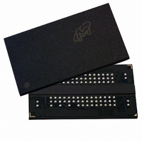
MT47H256M4BT-5E:A TR Micron Technology Inc, MT47H256M4BT-5E:A TR Datasheet - Page 41

MT47H256M4BT-5E:A TR
Manufacturer Part Number
MT47H256M4BT-5E:A TR
Description
IC DDR2 SDRAM 1GBIT 5NS 92FBGA
Manufacturer
Micron Technology Inc
Datasheet
1.MT47H256M4HQ-5EE_TR.pdf
(131 pages)
Specifications of MT47H256M4BT-5E:A TR
Format - Memory
RAM
Memory Type
DDR2 SDRAM
Memory Size
1G (256M x 4)
Speed
5ns
Interface
Parallel
Voltage - Supply
1.7 V ~ 1.9 V
Operating Temperature
0°C ~ 85°C
Package / Case
92-FBGA
Lead Free Status / RoHS Status
Lead free / RoHS Compliant
Other names
557-1206-1
- Current page: 41 of 131
- Download datasheet (10Mb)
AC and DC Operating Conditions
Table 12: Recommended DC Operating Conditions (SSTL_18)
All voltages referenced to V
PDF: 09005aef821ae8bf
1GbDDR2.pdf – Rev. T 02/10 EN
Parameter
Supply voltage
V
I/O supply voltage
I/O reference voltage
I/O termination voltage (system)
DDL
supply voltage
Notes:
SS
46. ODT turn-on time
47. ODT turn-off time
48. Half-clock output parameters must be derated by the actual
49. The -187E maximum limit is 2 ×
50. Should use 8
1. V
2. V
3. V
4. V
5. V
duty cycle was 47/53,
+ 0.03, or 2.53, for
gins to turn on. ODT turn-on time
Both are measured from
turn off time
input clock jitter is present; this will result in each parameter becoming larger. The pa-
rameter
t
t
3 x
DC level of the same. Peak-to-peak noise (noncommon mode) on V
±1 percent of the DC value. Peak-to-peak AC noise on V
of V
resistors, is expected to be set equal to V
V
JITdty (MAX). The parameter
ERR
DD
SSQ
DDQ
REF
TT
REF
t
is not applied directly to the device. V
CK +
REF(DC)
.
and V
5per
is expected to equal V
= V
tracks with V
(MIN) and
SSL
t
AOF (MIN) is required to be derated by subtracting both
t
AC (MAX) + 1000 in the future.
. This measurement is to be taken at the nearest V
Symbol
DDQ
V
= V
V
V
REF(DC)
V
V
t
DDQ
t
DDL
CK for backward compatibility.
DD
AOF (MAX) is when the bus is in High-Z. Both are measured from
TT
must track each other. V
SS
.
t
DD
t
t
t
AON (MIN) is when the device leaves High-Z and ODT resistance be-
AOF (MIN) is when the device starts to turn off ODT resistance. ODT
AOF (MAX).
JITdty (MIN).
; V
t
AOFD would actually be 2.5 - 0.03, or 2.47, for
0.49 × V
V
DDL
REF(DC)
t
AOND.
41
Min
DDQ
1.7
1.7
1.7
tracks with V
t
/2 of the transmitting device and to track variations in the
AOF (MAX) is required to be derated by subtracting both
- 40
DDQ
t
CK +
t
AON (MAX) is when the ODT resistance is fully on.
Micron Technology, Inc. reserves the right to change products or specifications without notice.
t
AC (MAX) + 1000 but it will likely be
DDQ
0.50 × V
DD
AC and DC Operating Conditions
REF
V
TT
Nom
.
REF(DC)
must be ≤ V
, and must track variations in the DC level of
1.8
1.8
1.8
is a system supply for signal termination
1Gb: x4, x8, x16 DDR2 SDRAM
DDQ
DD
V
REF
0.51 × V
REF(DC)
.
may not exceed ±2 percent
Max
1.9
1.9
1.9
REF
t
© 2004 Micron Technology, Inc. All rights reserved.
ERR
bypass capacitor.
+ 40
DDQ
5per
t
ERR
REF
t
and
AOF (MIN) and 2.5
may not exceed
5per
Units
mV
t
V
V
V
V
JITdty when
(MAX) and
t
AOFD.
Notes
1, 2
2, 3
2, 3
4
5
Related parts for MT47H256M4BT-5E:A TR
Image
Part Number
Description
Manufacturer
Datasheet
Request
R

Part Number:
Description:
IC DDR2 SDRAM 1GBIT 92FBGA
Manufacturer:
Micron Technology Inc
Datasheet:

Part Number:
Description:
IC DDR2 SDRAM 1GBIT 3NS 92FBGA
Manufacturer:
Micron Technology Inc
Datasheet:

Part Number:
Description:
IC DDR2 SDRAM 1GBIT 5NS 92FBGA
Manufacturer:
Micron Technology Inc
Datasheet:

Part Number:
Description:
IC SDRAM 64MBIT 133MHZ 54TSOP
Manufacturer:
Micron Technology Inc
Datasheet:

Part Number:
Description:
IC SDRAM 64MBIT 5.5NS 86TSOP
Manufacturer:
Micron Technology Inc
Datasheet:

Part Number:
Description:
IC SDRAM 64MBIT 200MHZ 86TSOP
Manufacturer:
Micron Technology Inc
Datasheet:

Part Number:
Description:
IC SDRAM 64MBIT 133MHZ 54TSOP
Manufacturer:
Micron Technology Inc
Datasheet:

Part Number:
Description:
IC SDRAM 128MBIT 133MHZ 54TSOP
Manufacturer:
Micron Technology Inc
Datasheet:

Part Number:
Description:
IC SDRAM 256MBIT 133MHZ 90VFBGA
Manufacturer:
Micron Technology Inc
Datasheet:

Part Number:
Description:
IC SDRAM 128MBIT 133MHZ 54TSOP
Manufacturer:
Micron Technology Inc
Datasheet:

Part Number:
Description:
IC SDRAM 256MBIT 133MHZ 54TSOP
Manufacturer:
Micron Technology Inc
Datasheet:

Part Number:
Description:
IC DDR SDRAM 512MBIT 6NS 66TSOP
Manufacturer:
Micron Technology Inc
Datasheet:

Part Number:
Description:
IC SDRAM 128MBIT 167MHZ 86TSOP
Manufacturer:
Micron Technology Inc
Datasheet:

Part Number:
Description:
IC SDRAM 128MBIT 143MHZ 86TSOP
Manufacturer:
Micron Technology Inc
Datasheet:

Part Number:
Description:
SDRAM 256M-BIT 1.8V 54-PIN VFBGA
Manufacturer:
Micron Technology Inc
Datasheet:


