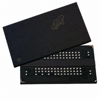
MT47H256M4BT-5E:A TR Micron Technology Inc, MT47H256M4BT-5E:A TR Datasheet - Page 78

MT47H256M4BT-5E:A TR
Manufacturer Part Number
MT47H256M4BT-5E:A TR
Description
IC DDR2 SDRAM 1GBIT 5NS 92FBGA
Manufacturer
Micron Technology Inc
Datasheet
1.MT47H256M4HQ-5EE_TR.pdf
(131 pages)
Specifications of MT47H256M4BT-5E:A TR
Format - Memory
RAM
Memory Type
DDR2 SDRAM
Memory Size
1G (256M x 4)
Speed
5ns
Interface
Parallel
Voltage - Supply
1.7 V ~ 1.9 V
Operating Temperature
0°C ~ 85°C
Package / Case
92-FBGA
Lead Free Status / RoHS Status
Lead free / RoHS Compliant
Other names
557-1206-1
- Current page: 78 of 131
- Download datasheet (10Mb)
CAS Latency (CL)
Figure 36: CL
PDF: 09005aef821ae8bf
1GbDDR2.pdf – Rev. T 02/10 EN
Notes:
The CAS latency (CL) is defined by bits M4–M6, as shown in Figure 35 (page 75). CL is
the delay, in clock cycles, between the registration of a READ command and the availa-
bility of the first bit of output data. The CL can be set to 3, 4, 5, 6, or 7 clocks, depending
on the speed grade option being used.
DDR2 SDRAM does not support any half-clock latencies. Reserved states should not be
used as an unknown operation otherwise incompatibility with future versions may result.
DDR2 SDRAM also supports a feature called posted CAS additive latency (AL). This fea-
ture allows the READ command to be issued prior to
internal command to the DDR2 SDRAM by AL clocks. The AL feature is described in
further detail in Posted CAS Additive Latency (AL) (page 81).
Examples of CL = 3 and CL = 4 are shown in Figure 36; both assume AL = 0. If a READ
command is registered at clock edge n, and the CL is m clocks, the data will be available
nominally coincident with clock edge n + m (this assumes AL = 0).
DQS, DQS#
DQS, DQS#
Command
Command
1. BL = 4.
2. Posted CAS# additive latency (AL) = 0.
3. Shown with nominal
CK#
CK#
DQ
DQ
CK
CK
READ
READ
T0
T0
NOP
NOP
T1
T1
CL = 3 (AL = 0)
t
AC,
78
t
DQSCK, and
CL = 4 (AL = 0)
NOP
NOP
T2
T2
Micron Technology, Inc. reserves the right to change products or specifications without notice.
t
DQSQ.
NOP
NOP
T3
T3
1Gb: x4, x8, x16 DDR2 SDRAM
DO
n
t
RCD (MIN) by delaying the
n + 1
DO
NOP
NOP
T4
T4
Mode Register (MR)
n + 2
DO
DO
n
© 2004 Micron Technology, Inc. All rights reserved.
Transitioning data
n + 1
n + 3
DO
DO
NOP
NOP
T5
T5
n + 2
DO
n + 3
DO
NOP
NOP
Don’t care
T6
T6
Related parts for MT47H256M4BT-5E:A TR
Image
Part Number
Description
Manufacturer
Datasheet
Request
R

Part Number:
Description:
IC DDR2 SDRAM 1GBIT 92FBGA
Manufacturer:
Micron Technology Inc
Datasheet:

Part Number:
Description:
IC DDR2 SDRAM 1GBIT 3NS 92FBGA
Manufacturer:
Micron Technology Inc
Datasheet:

Part Number:
Description:
IC DDR2 SDRAM 1GBIT 5NS 92FBGA
Manufacturer:
Micron Technology Inc
Datasheet:

Part Number:
Description:
IC SDRAM 64MBIT 133MHZ 54TSOP
Manufacturer:
Micron Technology Inc
Datasheet:

Part Number:
Description:
IC SDRAM 64MBIT 5.5NS 86TSOP
Manufacturer:
Micron Technology Inc
Datasheet:

Part Number:
Description:
IC SDRAM 64MBIT 200MHZ 86TSOP
Manufacturer:
Micron Technology Inc
Datasheet:

Part Number:
Description:
IC SDRAM 64MBIT 133MHZ 54TSOP
Manufacturer:
Micron Technology Inc
Datasheet:

Part Number:
Description:
IC SDRAM 128MBIT 133MHZ 54TSOP
Manufacturer:
Micron Technology Inc
Datasheet:

Part Number:
Description:
IC SDRAM 256MBIT 133MHZ 90VFBGA
Manufacturer:
Micron Technology Inc
Datasheet:

Part Number:
Description:
IC SDRAM 128MBIT 133MHZ 54TSOP
Manufacturer:
Micron Technology Inc
Datasheet:

Part Number:
Description:
IC SDRAM 256MBIT 133MHZ 54TSOP
Manufacturer:
Micron Technology Inc
Datasheet:

Part Number:
Description:
IC DDR SDRAM 512MBIT 6NS 66TSOP
Manufacturer:
Micron Technology Inc
Datasheet:

Part Number:
Description:
IC SDRAM 128MBIT 167MHZ 86TSOP
Manufacturer:
Micron Technology Inc
Datasheet:

Part Number:
Description:
IC SDRAM 128MBIT 143MHZ 86TSOP
Manufacturer:
Micron Technology Inc
Datasheet:

Part Number:
Description:
SDRAM 256M-BIT 1.8V 54-PIN VFBGA
Manufacturer:
Micron Technology Inc
Datasheet:


